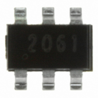
ZXTC2061E6TA Diodes Zetex, ZXTC2061E6TA Datasheet

ZXTC2061E6TA
Specifications of ZXTC2061E6TA
Related parts for ZXTC2061E6TA
ZXTC2061E6TA Summary of contents
Page 1
... Very low saturation voltage • High gain • SOT23-6 package Applications • MOSFET and IGBT gate driving • Motor drive Ordering information DEVICE Reel size (inches) ZXTC2061E6TA Device marking 2061 Issue 1 - November 2007 © Zetex Semiconductors plc 2007 device. Tape width Quantity (mm) per reel ...
Page 2
Absolute maximum and thermal ratings PARAMETER Collector-base voltage Collector-emitter voltage Emitter-base voltage Continuous collector current Peak pulse current Base current Power dissipation at T =25°C A Linear derating factor Power dissipation at T =25°C A Linear derating factor Power dissipation ...
Page 3
Thermal characteristics Issue 1 - November 2007 © Zetex Semiconductors plc 2007 ZXTC2061E6 3 www.zetex.com ...
Page 4
ELECTRICAL CHARACTERISTICS (at Tamb = 25°C unless otherwise stated). Parameter Symbol Collector-base BV breakdown voltage Collector-emitter BV breakdown voltage (base open) Emitter-base BV breakdown voltage Collector-base cut-off I CBO current Emitter-base cut-off I EBO current Collector-emitter V CE(sat) saturation voltage ...
Page 5
NPN electrical characteristics Issue 1 - November 2007 © Zetex Semiconductors plc 2007 ZXTC2061E6 5 www.zetex.com ...
Page 6
PNP electrical characteristics Issue 1 - November 2007 © Zetex Semiconductors plc 2007 ZXTC2061E6 6 www.zetex.com ...
Page 7
Package outline SOT23-6 Package outline DIM Min. A 0.90 A1 0.00 A2 0.90 b 0.35 C 0.09 D 2.70 E 2.20 E1 1. 0° Note: Controlling dimensions are in millimeters. Approximate dimensions are provided in ...
Page 8
Definitions Product change Zetex Semiconductors reserves the right to alter, without notice, specifications, design, price or conditions of supply of any product or service. Customers are solely responsible for obtaining the latest relevant information before placing orders. Applications disclaimer The ...


