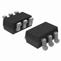
BC847CDW1T1G ON Semiconductor, BC847CDW1T1G Datasheet - Page 9

BC847CDW1T1G
Manufacturer Part Number
BC847CDW1T1G
Description
TRANS NPN DUAL 45V 100MA SOT-363
Manufacturer
ON Semiconductor
Datasheet
1.BC846BDW1T1G.pdf
(10 pages)
Specifications of BC847CDW1T1G
Transistor Type
2 NPN (Dual)
Current - Collector (ic) (max)
100mA
Voltage - Collector Emitter Breakdown (max)
45V
Vce Saturation (max) @ Ib, Ic
600mV @ 5mA, 100mA
Dc Current Gain (hfe) (min) @ Ic, Vce
420 @ 2mA, 5V
Power - Max
380mW
Frequency - Transition
100MHz
Mounting Type
Surface Mount
Package / Case
SC-70-6, SC-88, SOT-363
Configuration
Dual
Transistor Polarity
NPN
Mounting Style
SMD/SMT
Collector- Emitter Voltage Vceo Max
45 V
Emitter- Base Voltage Vebo
6 V
Continuous Collector Current
0.1 A
Maximum Dc Collector Current
0.1 A
Power Dissipation
380 mW
Maximum Operating Frequency
100 MHz
Maximum Operating Temperature
+ 150 C
Dc Collector/base Gain Hfe Min
420 at 2 mA at 5 V
Minimum Operating Temperature
- 55 C
Number Of Elements
2
Collector-emitter Voltage
45V
Collector-base Voltage
50V
Emitter-base Voltage
6V
Collector Current (dc) (max)
100mA
Dc Current Gain (min)
420
Frequency (max)
100MHz
Operating Temp Range
-55C to 150C
Operating Temperature Classification
Military
Mounting
Surface Mount
Pin Count
6
Package Type
SC-88
Lead Free Status / RoHS Status
Lead free / RoHS Compliant
Current - Collector Cutoff (max)
-
Lead Free Status / Rohs Status
Lead free / RoHS Compliant
Other names
BC847CDW1T1G
BC847CDW1T1GOSTR
BC847CDW1T1GOSTR
Available stocks
Company
Part Number
Manufacturer
Quantity
Price
Company:
Part Number:
BC847CDW1T1G
Manufacturer:
ON Semiconductor
Quantity:
4 500
Company:
Part Number:
BC847CDW1T1G
Manufacturer:
ON
Quantity:
30 000
Part Number:
BC847CDW1T1G
Manufacturer:
ON/安森美
Quantity:
20 000
†For information on tape and reel specifications, including part orientation and tape sizes, please refer to our Tape and Reel Packaging
ORDERING INFORMATION
Specifications Brochure, BRD8011/D.
BC846BDW1T1G
BC847BDW1T1G
BC847BDW1T3G
BC847CDW1T1G
BC848CDW1T1G
-200
-100
-5.0
-2.0
-50
-10
0.001
0.01
1.0
0.1
-1.0
0
Figure 35. Active Region Safe Operating Area
0.02
0.05
0.01
D = 0.5
0.2
0.1
SINGLE PULSE
Device
V
CE
, COLLECTOR-EMITTER VOLTAGE (V)
BONDING WIRE LIMIT
THERMAL LIMIT
SECOND BREAKDOWN LIMIT
-5.0
T
1.0
A
= 25°C
-10
T
BC558
BC557
BC556
J
1 s
= 25°C
Markings
10
-30 -45 -65 -100
1G
1B
1F
1F
1L
Figure 34. Thermal Response
3 ms
http://onsemi.com
t, TIME (ms)
100
9
of the transistor that must be observed for reliable
operation. Collector load lines for specific circuits must
fall below the limits indicated by the applicable curve.
or T
curves are valid for duty cycles to 10% provided T
150°C. T
Figure 34. At high case or ambient temperatures,
thermal limitations will reduce the power that can be
handled to values less than the limitations imposed by the
secondary breakdown.
P
(pk)
The safe operating area curves indicate I
The data of Figure 35 is based upon T
DUTY CYCLE, D = t
A
(Pb−Free)
(Pb−Free)
(Pb−Free)
(Pb−Free)
(Pb−Free)
SOT−363
SOT−363
SOT−363
SOT−363
SOT−363
Package
is variable depending upon conditions. Pulse
1.0 k
t
1
J(pk)
t
2
may be calculated from the data in
1
/t
2
10 k
Z
R
D CURVES APPLY FOR POWER
PULSE TRAIN SHOWN
READ TIME AT t
T
qJA
J(pk)
qJA
(t) = r(t) R
= 3285C/W MAX
10000 / Tape & Reel
− T
3000 / Tape & Reel
3000 / Tape & Reel
3000 / Tape & Reel
3000 / Tape & Reel
C
= P
Shipping
qJA
(pk)
J(pk)
100 k
1
R
qJC
C
= 150°C; T
(t)
−V
†
CE
J(pk)
limits
1.0 M
C
≤


