NST3904DXV6T5G ON Semiconductor, NST3904DXV6T5G Datasheet - Page 2
NST3904DXV6T5G
Manufacturer Part Number
NST3904DXV6T5G
Description
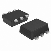
TRANS NPN DUAL 200MA 40V SOT563
Manufacturer
ON Semiconductor
Datasheet
1.NST3904DXV6T1G.pdf
(6 pages)
Specifications of NST3904DXV6T5G
Transistor Type
2 NPN (Dual)
Current - Collector (ic) (max)
200mA
Voltage - Collector Emitter Breakdown (max)
40V
Vce Saturation (max) @ Ib, Ic
300mV @ 5mA, 50mA
Dc Current Gain (hfe) (min) @ Ic, Vce
100 @ 10mA, 1V
Power - Max
500mW
Frequency - Transition
300MHz
Mounting Type
Surface Mount
Package / Case
SOT-563, SOT-6
Lead Free Status / RoHS Status
Lead free / RoHS Compliant
Current - Collector Cutoff (max)
-
Other names
NST3904DXV6T5GOS
NST3904DXV6T5GOS
NST3904DXV6T5GOSTR
NST3904DXV6T5GOS
NST3904DXV6T5GOSTR
Available stocks
Company
Part Number
Manufacturer
Quantity
Price
Company:

Part Number:
NST3904DXV6T5G
Manufacturer:
ON Semiconductor
Quantity:
47 000
Company:
Part Number:
NST3904DXV6T5G
Manufacturer:
ON Semiconductor
Quantity:
5 700
Company:
Part Number:
NST3904DXV6T5G
Manufacturer:
ON
Quantity:
30 000


2. Pulse Test: Pulse Width ≤ 300 ms; Duty Cycle ≤ 2.0%.
Figure 1. Delay and Rise Time Equivalent Test Circuit
- 0.5 V
ELECTRICAL CHARACTERISTICS
OFF CHARACTERISTICS
ON CHARACTERISTICS (Note 2)
SMALL-SIGNAL CHARACTERISTICS
SWITCHING CHARACTERISTICS
Collector - Emitter Breakdown Voltage (Note 2) (I
Collector - Base Breakdown Voltage (I
Emitter - Base Breakdown Voltage (I
Base Cutoff Current (V
Collector Cutoff Current (V
DC Current Gain
Collector - Emitter Saturation Voltage
Base - Emitter Saturation Voltage
Current - Gain - Bandwidth Product (I
Output Capacitance (V
Input Capacitance (V
Input Impedance (V
Voltage Feedback Ratio (V
Small - Signal Current Gain (V
Output Admittance (V
Noise Figure (V
Delay Time
Rise Time
Storage Time
Fall Time
DUTY CYCLE = 2%
300 ns
(I
(I
(I
(I
(I
(I
(I
(I
(I
C
C
C
C
C
C
C
C
C
= 0.1 mAdc, V
= 1.0 mAdc, V
= 10 mAdc, V
= 50 mAdc, V
= 100 mAdc, V
= 10 mAdc, I
= 50 mAdc, I
= 10 mAdc, I
= 50 mAdc, I
CE
= 5.0 Vdc, I
B
B
B
B
CE
CE
CE
CE
CE
EB
= 1.0 mAdc)
= 5.0 mAdc)
= 1.0 mAdc)
= 5.0 mAdc)
CE
CE
+10.9 V
CE
CB
= 10 Vdc, I
= 1.0 Vdc)
= 1.0 Vdc)
< 1 ns
= 1.0 Vdc)
= 1.0 Vdc)
= 0.5 Vdc, I
= 10 Vdc, I
= 1.0 Vdc)
= 30 Vdc, V
= 5.0 Vdc, I
CE
CE
= 30 Vdc, V
= 10 Vdc, I
CE
C
10 k
= 100 mAdc, R
= 10 Vdc, I
C
C
C
= 1.0 mAdc, f = 1.0 kHz)
E
Characteristic
C
E
= 1.0 mAdc, f = 1.0 kHz)
EB
= 0, f = 1.0 MHz)
C
= 10 mAdc, I
= 0, f = 1.0 MHz)
= 10 mAdc, V
= 10 mAdc, I
= 3.0 Vdc)
C
NST3904DXV6T1, NST3904DXV6T5
(V
(I
(V
(I
(T
EB
C
B1
= 1.0 mAdc, f = 1.0 kHz)
* Total shunt capacitance of test jig and connectors
A
CC
CC
C
= 3.0 Vdc)
= 10 mAdc, I
= 25°C unless otherwise noted)
= I
= 1.0 mAdc, f = 1.0 kHz)
+3 V
S
= 3.0 Vdc, V
= 3.0 Vdc, I
B2
C
= 1.0 k W, f = 1.0 kHz)
C
= 1.0 mAdc, I
= 1.0 mAdc)
E
= 0)
275
CE
= 0)
C
s
= 20 Vdc, f = 100 MHz)
< 4 pF*
http://onsemi.com
B1
C
BE
= 1.0 mAdc)
= 10 mAdc)
= - 0.5 Vdc)
B
DUTY CYCLE = 2%
= 0)
2
10 < t
Figure 2. Storage and Fall Time Equivalent Test Circuit
1
< 500 ms
0
- 9.1 V′
t
1
V
V
V
+10.9 V
Symbol
V
V
(BR)CEO
(BR)CBO
(BR)EBO
CE(sat)
BE(sat)
C
I
C
h
h
< 1 ns
CEX
NF
I
h
h
h
BL
f
t
t
obo
t
FE
t
T
ibo
oe
re
fe
d
s
ie
r
f
1N916
10 k
0.65
Min
100
300
100
100
6.0
1.0
2.0
0.5
0.1
1.0
3.0
40
60
40
70
60
30
-
-
-
-
-
-
-
-
-
-
-
-
-
Max
0.85
0.95
300
400
400
200
0.2
0.3
4.0
8.0
8.0
5.0
4.0
50
50
10
12
10
40
60
35
35
50
-
-
-
-
-
-
-
-
+3 V
C
275
mmhos
X 10
nAdc
nAdc
s
MHz
Unit
Vdc
Vdc
Vdc
Vdc
Vdc
k W
< 4 pF*
dB
pF
pF
ns
ns
-
-
- 4
Related parts for NST3904DXV6T5G
Image
Part Number
Description
Manufacturer
Datasheet
Request
R

Part Number:
Description:
ON Semiconductor [VOLTAGE REGULATOR]
Manufacturer:
ON Semiconductor
Datasheet:
Part Number:
Description:
357-036-542-201 CARDEDGE 36POS DL .156 BLK LOPRO
Manufacturer:
ON Semiconductor
Datasheet:
Part Number:
Description:
357-036-542-201 CARDEDGE 36POS DL .156 BLK LOPRO
Manufacturer:
ON Semiconductor
Datasheet:
Part Number:
Description:
357-036-542-201 CARDEDGE 36POS DL .156 BLK LOPRO
Manufacturer:
ON Semiconductor
Datasheet:
Part Number:
Description:
357-036-542-201 CARDEDGE 36POS DL .156 BLK LOPRO
Manufacturer:
ON Semiconductor
Datasheet:
Part Number:
Description:
357-036-542-201 CARDEDGE 36POS DL .156 BLK LOPRO
Manufacturer:
ON Semiconductor
Datasheet:
Part Number:
Description:
357-036-542-201 CARDEDGE 36POS DL .156 BLK LOPRO
Manufacturer:
ON Semiconductor
Datasheet:
Part Number:
Description:
357-036-542-201 CARDEDGE 36POS DL .156 BLK LOPRO
Manufacturer:
ON Semiconductor
Datasheet:
Part Number:
Description:
357-036-542-201 CARDEDGE 36POS DL .156 BLK LOPRO
Manufacturer:
ON Semiconductor
Datasheet:
Part Number:
Description:
357-036-542-201 CARDEDGE 36POS DL .156 BLK LOPRO
Manufacturer:
ON Semiconductor
Datasheet:
Part Number:
Description:
357-036-542-201 CARDEDGE 36POS DL .156 BLK LOPRO
Manufacturer:
ON Semiconductor
Datasheet:
Part Number:
Description:
Manufacturer:
ON Semiconductor
Datasheet:
Part Number:
Description:
Manufacturer:
ON Semiconductor
Datasheet:
Part Number:
Description:
Manufacturer:
ON Semiconductor
Datasheet: