MAT02FH Analog Devices Inc, MAT02FH Datasheet - Page 6
MAT02FH
Manufacturer Part Number
MAT02FH
Description
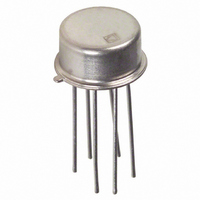
IC TRANS DUAL MATCHED NPN TO78-6
Manufacturer
Analog Devices Inc
Datasheet
1.MAT02EH.pdf
(12 pages)
Specifications of MAT02FH
Transistor Type
2 NPN (Dual)
Current - Collector (ic) (max)
20mA
Voltage - Collector Emitter Breakdown (max)
40V
Vce Saturation (max) @ Ib, Ic
200mV @ 100µA, 1mA
Current - Collector Cutoff (max)
4nA
Power - Max
1.8W
Frequency - Transition
200MHz
Mounting Type
Through Hole
Package / Case
TO-78-6 Metal Can
Lead Free Status / RoHS Status
Contains lead / RoHS non-compliant
Dc Current Gain (hfe) (min) @ Ic, Vce
-
Available stocks
Company
Part Number
Manufacturer
Quantity
Price


MAT02
LOG CONFORMANCE TESTING
The log conformance of the MAT02 is tested using the circuit
shown above. The circuit employs a dual transdiode logarithmic
converter operating at a fixed ratio of collector currents that are
swept over a 10:1 range. The output of each transdiode converter
is the V
uct of the collector current and r
The difference of the V
AMP01 instrumentation amplifier. The differential emitter-base
voltage (∆V
an ac error voltage, which is the deviation from true log confor-
mity as the collector currents vary.
The output of the transdiode logarithmic converter comes from
the idealized intrinsic transistor equation (for silicon):
where
k = Boltzmann’s Constant (1.38062 × 10
q = Unit Electron Charge (1.60219 × 10
T = Absolute Temperature, K (= °C + 273.2)
I
I
An error term must be added to this equation to allow for the
bulk resistance (r
input current is limited by use of the OP15 BiFET-input op
amp. The resulting AMP01 input is:
S
C
= Extrapolated Current for V
= Collector Current
BE
of the transistor plus an error term which is the prod-
BE
) consists of a temperature-dependent dc level plus
V
BE
BE
=
) of the transistor. Error due to the op amp
kT
q
BE
In
is amplified at a gain of ×100 by the
I
I
C
S
BE
BE
→0
, the bulk emitter resistance.
–19
–23
°C)
J/K)
Figure 1. Log Conformance Test Circuit
(1)
–6–
A ramp function that sweeps from 1 V to 10 V is converted by
the op amps to a collector current ramp through each transistor.
Because I
the previous equation becomes:
As viewed on an oscilloscope, the change in ∆V
change in I
With the oscilloscope ac coupled, the temperature dependent
term becomes a dc offset and the trace represents the deviation
from true log conformity. The bulk resistance can be calculated
from the voltage deviation ∆V
current (9 mA):
This procedure finds r
provide the r
R
1
= R
2
.
∆ V
∆ V
C1
C
BE
BE
is made equal to 10 I
BE
is then displayed as shown in Figure 2 below:
=
= 59 mV + 0.9 I
for Side B. Differential r
kT
r
q
BE
In
=
BE
I
I
9 mA
∆V
C2
C1
for Side A. Switching R
+ I
Figure 2.
O
×
O
C1
C1
100
and the change in collector
r
1
BE1
C2
r
BE
, and assuming T
– I
( ∆ r
C2
BE
BE
r
is found by making
BE2
~ 0)
BE
1
for a 10:1
and R
A
= 25°C,
2
REV. E
will
(2)
(3)
Related parts for MAT02FH
Image
Part Number
Description
Manufacturer
Datasheet
Request
R

Part Number:
Description:
±1.7g Dual-Axis IMEMS Accelerometer Evaluation Board
Manufacturer:
Analog Devices Inc
Datasheet:

Part Number:
Description:
Inertial Sensor Evaluation System
Manufacturer:
Analog Devices Inc
Datasheet:
Part Number:
Description:
Manufacturer:
Analog Devices Inc
Datasheet:
Part Number:
Description:
Manufacturer:
Analog Devices Inc
Datasheet:
Part Number:
Description:
Manufacturer:
Analog Devices Inc
Datasheet:
Part Number:
Description:
Manufacturer:
Analog Devices Inc
Datasheet:
Part Number:
Description:
Manufacturer:
Analog Devices Inc
Datasheet:
Part Number:
Description:
Manufacturer:
Analog Devices Inc
Datasheet:
Part Number:
Description:
Manufacturer:
Analog Devices Inc
Datasheet:
Part Number:
Description:
Manufacturer:
Analog Devices Inc
Datasheet:
Part Number:
Description:
Manufacturer:
Analog Devices Inc
Datasheet:
Part Number:
Description:
Manufacturer:
Analog Devices Inc
Datasheet:
Part Number:
Description:
Manufacturer:
Analog Devices Inc
Datasheet: