74HC4060PW-T NXP Semiconductors, 74HC4060PW-T Datasheet
74HC4060PW-T
Specifications of 74HC4060PW-T


74HC4060PW-T Summary of contents
Page 1
... RC or crystal oscillator configuration I Complies with JEDEC standard no ESD protection: N HBM JESD22-A114E exceeds 2000 JESD22-A115-A exceeds 200 V I Multiple package options I Specified from +85 C and from +125 C 3. Applications I Control counters I Timers I Frequency dividers I Time-delay circuits . CC Product data sheet ...
Page 2
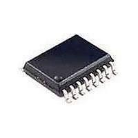
... Ordering information Type number Package Temperature range Name 74HC4060N +125 C 74HCT4060N 74HC4060D +125 C 74HCT4060D 74HC4060DB +125 C 74HCT4060DB 74HC4060PW +125 C 74HC4060BQ +125 C 74HCT4060BQ 5. Functional diagram Fig 1. Logic symbol 74HC_HCT4060_3 Product data sheet 74HC4060; 74HCT4060 14-stage binary ripple counter with oscillator Description DIP16 plastic dual in-line package ...
Page 3
... NXP Semiconductors Fig 2. IEC logic symbol Fig 3. Functional diagram CTC RTC RS MR Fig 4. Logic diagram 74HC_HCT4060_3 Product data sheet 74HC4060; 74HCT4060 14-stage binary ripple counter with oscillator CTR14 AND RCX ( RTC CTC CP 14-STAGE BINARY COUNTER Rev. 03 — 14 July 2008 CTR14 (b) 001aai468 ...
Page 4
... NXP Semiconductors 6. Pinning information 6.1 Pinning 74HC4060 74HCT4060 Q11 1 2 Q12 Q13 GND 001aai115 Fig 5. Pin configuration DIP16, SO16 and (T)SSOP16 6.2 Pin description Table 2. Pin description Symbol Pin Q11 to Q13 14, 13, 15 GND 8 CTC 9 RTC 74HC_HCT4060_3 Product data sheet 74HC4060; 74HCT4060 ...
Page 5
... NXP Semiconductors 7. Functional description Q11 Q12 Q13 Fig 7. Timing diagram 8. Limiting values Table 3. Limiting values In accordance with the Absolute Maximum Rating System (IEC 60134). Voltages are referenced to GND (ground = 0 V). Symbol Parameter V supply voltage CC I input clamping current IK I output clamping current ...
Page 6
... NXP Semiconductors Table 3. Limiting values …continued In accordance with the Absolute Maximum Rating System (IEC 60134). Voltages are referenced to GND (ground = 0 V). Symbol Parameter P total power dissipation tot [1] The input and output voltage ratings may be exceeded if the input and output current ratings are observed. ...
Page 7
... NXP Semiconductors Table 5. Static characteristics At recommended operating conditions; voltages are referenced to GND (ground = 0 V). Symbol Parameter Conditions V LOW-level MR input IL input voltage input HIGH-level RTC output GND OH output voltage 2.6 mA 3.3 mA RTC output 0.65 mA 0.85 mA CTC output 3.2 mA; V ...
Page 8
... NXP Semiconductors Table 5. Static characteristics At recommended operating conditions; voltages are referenced to GND (ground = 0 V). Symbol Parameter Conditions V LOW-level RTC output output MR = GND voltage 2.6 mA 3.3 mA CTC output 3.2 mA 4.2 mA except RTC output except RTC and CTC outputs I = 4.0 mA 5.2 mA input leakage ...
Page 9
... NXP Semiconductors Table 5. Static characteristics At recommended operating conditions; voltages are referenced to GND (ground = 0 V). Symbol Parameter Conditions V HIGH-level RTC output output voltage I = 0.65 mA RTC output GND 2.6 mA CTC output 3.2 mA except RTC output except RTC and CTC outputs I = 4.0 mA LOW-level RTC output ...
Page 10
... NXP Semiconductors 11. Dynamic characteristics Table 6. Dynamic characteristics GND = unless otherwise specified; for test circuit see L Symbol Parameter Conditions 74HC4060 t propagation RS to Q3; see pd delay Qn+1; see HIGH to LOW MR to Qn; see PHL propagation V CC delay transition time Qn; see pulse width RS (HIGH or LOW); ...
Page 11
... NXP Semiconductors Table 6. Dynamic characteristics GND = unless otherwise specified; for test circuit see L Symbol Parameter Conditions f maximum RS; see max frequency power V = GND dissipation capacitance 74HCT4060 t propagation RS to Q3; see pd delay Qn+1; see HIGH to LOW MR to Qn; see PHL propagation V CC delay transition time Qn ...
Page 12
... NXP Semiconductors Table 6. Dynamic characteristics GND = unless otherwise specified; for test circuit see L Symbol Parameter Conditions C power V = GND dissipation capacitance [ the same as t and PHL PLH [2] Qn+1 is the next Qn output. [ the same as t and THL TLH [ used to determine the dynamic power dissipation (P ...
Page 13
... NXP Semiconductors Qn+1 output Measurement points are given in V and V are typical voltage output levels that occur with the output load Fig 9. Waveforms showing the output Qn to output Qn+1 propagation delays MR input Qn output Measurement points are given in V and V are typical voltage output levels that occur with the output load. ...
Page 14
... NXP Semiconductors Test data is given in Table 8. Definitions test circuit Termination resistance should be equal to output impedance Load capacitance including jig and probe capacitance. L Fig 11. Test circuit for measuring switching times Table 8. Test data Type Input V I 74HC4060 V CC 74HCT4060 3 V 74HC_HCT4060_3 Product data sheet 74HC4060 ...
Page 15
... NXP Semiconductors 13. RC oscillator 13.1 Timing component limitations The oscillator frequency is mainly determined by R R2C2 << R across the input protection diodes on the frequency. The stray capacitance C2 should be kept as small as possible. In consideration of accuracy, C stray capacitance. R typically is 280 Fig 12. Example oscillator The recommended values for these components to maintain agreement with the typical ...
Page 16
... NXP Semiconductors MR (from logic Rbias 100 Fig 13. External component connection for a crystal oscillator amb (1) Maximum. (2) Typical. (3) Minimum. Fig 15. Typical forward transconductance as function of the supply voltage 74HC_HCT4060_3 Product data sheet 74HC4060 74HCT4060 RTC 100 pF 001aai122 Fig 14. Test set-up for measuring forward ...
Page 17
... NXP Semiconductors osc R t ( amb For R curve nF Fig 16. RC oscillator frequency as a function of R 74HC_HCT4060_3 Product data sheet 001aai125 f (Hz Fig 17. RC oscillator frequency as a function Rev. 03 — 14 July 2008 74HC4060; 74HCT4060 14-stage binary ripple counter with oscillator 5 10 osc ...
Page 18
... NXP Semiconductors 14. Package outline DIP16: plastic dual in-line package; 16 leads (300 mil pin 1 index 1 DIMENSIONS (inch dimensions are derived from the original mm dimensions UNIT max. min. max. mm 4.2 0.51 3.2 inches 0.17 0.02 0.13 Note 1. Plastic or metal protrusions of 0.25 mm (0.01 inch) maximum per side are not included. ...
Page 19
... NXP Semiconductors SO16: plastic small outline package; 16 leads; body width 3 pin 1 index 1 DIMENSIONS (inch dimensions are derived from the original mm dimensions) A UNIT max. 0.25 1.45 mm 1.75 0.25 0.10 1.25 0.010 0.057 inches 0.069 0.01 0.004 0.049 Note 1. Plastic or metal protrusions of 0.15 mm (0.006 inch) maximum per side are not included. ...
Page 20
... NXP Semiconductors SSOP16: plastic shrink small outline package; 16 leads; body width 5 pin 1 index 1 e DIMENSIONS (mm are the original dimensions) A UNIT max. 0.21 1. 0.25 0.05 1.65 Note 1. Plastic or metal protrusions of 0.25 mm maximum per side are not included. OUTLINE VERSION IEC SOT338-1 Fig 20. Package outline SOT338-1 (SSOP16) ...
Page 21
... NXP Semiconductors TSSOP16: plastic thin shrink small outline package; 16 leads; body width 4 pin 1 index 1 DIMENSIONS (mm are the original dimensions) A UNIT max. 0.15 0.95 mm 1.1 0.25 0.05 0.80 Notes 1. Plastic or metal protrusions of 0.15 mm maximum per side are not included. 2. Plastic interlead protrusions of 0.25 mm maximum per side are not included. ...
Page 22
... NXP Semiconductors DHVQFN16: plastic dual in-line compatible thermal enhanced very thin quad flat package; no leads; 16 terminals; body 2.5 x 3.5 x 0.85 mm terminal 1 index area terminal 1 index area DIMENSIONS (mm are the original dimensions) (1) A UNIT max. 0.05 0. 0.2 0.00 0.18 Note 1. Plastic or metal protrusions of 0.075 mm maximum per side are not included. ...
Page 23
... Product data sheet Data sheet status Product data sheet • The format of this data sheet has been redesigned to comply with the new identity guidelines of NXP Semiconductors. • Legal texts have been adapted to the new company name where appropriate. • Section 4: DHVQFN16 package added. ...
Page 24
... Right to make changes — NXP Semiconductors reserves the right to make changes to information published in this document, including without limitation specifications and product descriptions, at any time and without notice ...
Page 25
... NXP Semiconductors 20. Contents 1 General description . . . . . . . . . . . . . . . . . . . . . . 1 2 Features . . . . . . . . . . . . . . . . . . . . . . . . . . . . . . . 1 3 Applications . . . . . . . . . . . . . . . . . . . . . . . . . . . . 1 4 Ordering information . . . . . . . . . . . . . . . . . . . . . 2 5 Functional diagram . . . . . . . . . . . . . . . . . . . . . . 2 6 Pinning information . . . . . . . . . . . . . . . . . . . . . . 4 6.1 Pinning . . . . . . . . . . . . . . . . . . . . . . . . . . . . . . . 4 6.2 Pin description . . . . . . . . . . . . . . . . . . . . . . . . . 4 7 Functional description . . . . . . . . . . . . . . . . . . . 5 8 Limiting values Recommended operating conditions Static characteristics Dynamic characteristics . . . . . . . . . . . . . . . . . 10 12 Waveforms . . . . . . . . . . . . . . . . . . . . . . . . . . . . oscillator 13.1 Timing component limitations . . . . . . . . . . . . . 15 13 ...