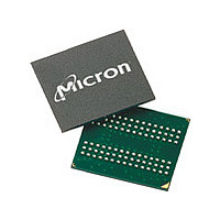
MT48LC4M32B2F5-7 IT:G Micron Technology Inc, MT48LC4M32B2F5-7 IT:G Datasheet - Page 36

MT48LC4M32B2F5-7 IT:G
Manufacturer Part Number
MT48LC4M32B2F5-7 IT:G
Description
DRAM Chip SDRAM 128M-Bit 4Mx32 3.3V 90-Pin VFBGA Tray
Manufacturer
Micron Technology Inc
Type
SDRAMr
Datasheet
1.MT48LC4M32B2F5-7_ITG.pdf
(67 pages)
Specifications of MT48LC4M32B2F5-7 IT:G
Density
128 Mb
Maximum Clock Rate
143 MHz
Package
90VFBGA
Address Bus Width
14 Bit
Operating Supply Voltage
3.3 V
Maximum Random Access Time
17|8|5.5 ns
Operating Temperature
-40 to 85 °C
Organization
4Mx32
Address Bus
14b
Access Time (max)
17/8/5.5ns
Operating Supply Voltage (typ)
3.3V
Package Type
VFBGA
Operating Temp Range
-40C to 85C
Operating Supply Voltage (max)
3.6V
Operating Supply Voltage (min)
3V
Supply Current
175mA
Pin Count
90
Mounting
Surface Mount
Operating Temperature Classification
Industrial
Lead Free Status / Rohs Status
Not Compliant
Figure 29:
Figure 30:
PDF: 09005aef80872800/Source: 09005aef80863355
128MbSDRAMx32_2.fm - Rev. L 1/09 EN
WRITE With Auto Precharge Interrupted by a READ
WRITE With Auto Precharge Interrupted by a WRITE
Notes:
Notes:
1. DQM is LOW.
1. DQM is LOW.
Internal
States
Internal
States
COMMAND
COMMAND
ADDRESS
ADDRESS
BANK m
BANK m
BANK n
BANK n
CLK
CLK
DQ
DQ
Page Active
Page Active
T0
NOP
T0
NOP
WRITE - AP
WRITE - AP
BANK n,
BANK n,
Page Active
Page Active
BANK n
BANK n
COL a
COL a
T1
T1
D
D
a
a
IN
IN
WRITE with Burst of 4
WRITE with Burst of 4
36
a + 1
a + 1
T2
T2
D
D
NOP
NOP
IN
IN
BANK m,
READ - AP
Micron Technology, Inc., reserves the right to change products or specifications without notice.
a + 2
T3
COL d
T3
BANK m
D
NOP
IN
Interrupt Burst, Write-Back
t
WR - BANK n
READ with Burst of 4
BANK m,
WRITE - AP
COL d
T4
T4
BANK m
CL = 3 (BANK m)
D
NOP
t
d
IN
Interrupt Burst, Write-Back
WR - BANK n
WRITE with Burst of 4
T5
T5
d + 1
NOP
NOP
D
IN
Precharge
t
RP - BANK n
T6
T6
d + 2
D
NOP
D
NOP
OUT
t RP - BANK n
d
IN
Precharge
©2001 Micron Technology, Inc. All rights reserved.
128Mb: x32 SDRAM
Register Definition
DON’T CARE
DON’T CARE
T7
T7
d + 3
D
d + 1
NOP
NOP
D
t WR - BANK m
OUT
t RP - BANK m
IN
Write-Back


