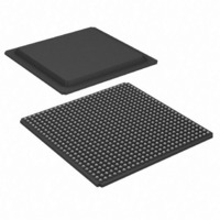
XC2V3000-4FGG676C Xilinx Inc, XC2V3000-4FGG676C Datasheet - Page 58

XC2V3000-4FGG676C
Manufacturer Part Number
XC2V3000-4FGG676C
Description
FPGA Virtex-II™ Family 3M Gates 32256 Cells 650MHz 0.15um/0.12um (CMOS) Technology 1.5V 676-Pin FBGA
Manufacturer
Xilinx Inc
Series
Virtex™-IIr
Datasheet
1.XC2V250-4FGG256C.pdf
(318 pages)
Specifications of XC2V3000-4FGG676C
Package
676FBGA
Family Name
Virtex-IIÂ
Device Logic Units
32256
Device System Gates
3000000
Number Of Registers
28672
Maximum Internal Frequency
650 MHz
Typical Operating Supply Voltage
1.5 V
Maximum Number Of User I/os
484
Ram Bits
1769472
Number Of Labs/clbs
3584
Total Ram Bits
1769472
Number Of I /o
484
Number Of Gates
3000000
Voltage - Supply
1.425 V ~ 1.575 V
Mounting Type
Surface Mount
Operating Temperature
0°C ~ 85°C
Package / Case
676-BBGA
Lead Free Status / RoHS Status
Lead free / RoHS Compliant
Number Of Logic Elements/cells
-
Lead Free Status / RoHS Status
Lead free / RoHS Compliant
Other names
122-1354
Available stocks
Company
Part Number
Manufacturer
Quantity
Price
Company:
Part Number:
XC2V3000-4FGG676C
Manufacturer:
XILINX
Quantity:
1 831
Company:
Part Number:
XC2V3000-4FGG676C
Manufacturer:
Xilinx Inc
Quantity:
10 000
- Current page: 58 of 318
- Download datasheet (3Mb)
Table 14: IOB Input Switching Characteristics (Continued)
DS031-3 (v3.5) November 5, 2007
Product Specification
Notes:
1. Input timing for LVTTL is measured at 1.4 V. For other I/O standards, see
Propagation Delays
Pad to output IQ via transparent
latch, no delay
Pad to output IQ via transparent
latch, with delay
Clock CLK to output IQ
Setup and Hold Times With Respect to Clock at IOB Input
Register
Pad, no delay
Pad, with delay
ICE input
SR input (IFF, synchronous)
Set/Reset Delays
SR input to IQ (asynchronous)
GSR to output IQ
Description
R
T
T
T
IOPICKD
IOICECK
IOPICK
Symbol
T
T
T
T
T
IOSRCKI
T
IOCKIQ
IOSRIQ
IOPLID
GSRQ
IOPLI
/T
/T
/T
IOICKP
IOICKPD
IOCKICE
www.xilinx.com
XC2V1000
XC2V1500
XC2V2000
XC2V3000
XC2V4000
XC2V6000
XC2V8000
XC2V1000
XC2V1500
XC2V2000
XC2V3000
XC2V4000
XC2V6000
XC2V8000
XC2V250
XC2V500
XC2V250
XC2V500
XC2V40
XC2V80
XC2V40
XC2V80
Device
Virtex-II Platform FPGAs: DC and Switching Characteristics
All
All
All
All
All
All
All
0.84/–0.36
3.24/–2.04
3.24/–2.04
3.24/–2.04
3.24/–2.04
3.24/–2.04
3.24/–2.04
3.24/–2.04
3.33/–2.10
3.33/–2.10
3.61/–2.29
Table
0.83
3.23
3.23
3.23
3.23
3.23
3.23
3.23
3.32
3.32
3.60
0.27
1.11
5.44
-6
18.
Speed Grade
0.92/–0.39
3.57/–2.24
3.57/–2.24
3.57/–2.24
3.57/–2.24
3.57/–2.24
3.57/–2.24
3.57/–2.24
3.67/–2.31
3.67/–2.31
3.97/–2.52
3.97/–2.52
0.21/ 0.04
0.91
3.55
3.55
3.55
3.55
3.55
3.55
3.55
3.65
3.65
3.95
3.95
0.67
0.30
1.22
5.98
-5
1.06/–0.45
4.10/–2.58
4.10/–2.58
4.10/–2.58
4.10/–2.58
4.10/–2.58
4.10/–2.58
4.10/–2.58
4.22/–2.66
4.22/–2.66
4.56/–2.90
4.56/–2.90
0.24/ 0.04
1.05
4.09
4.09
4.09
4.09
4.09
4.09
4.09
4.20
4.20
4.55
4.55
0.77
0.34
1.40
6.88
-4
ns, Max
ns, Max
ns, Max
ns, Max
ns, Max
ns, Max
ns, Max
ns, Max
ns, Max
ns, Max
ns, Max
ns, Max
ns, Max
ns, Max
ns, Max
ns, Min
ns, Min
ns, Min
ns, Min
ns, Min
ns, Min
ns, Min
ns, Min
ns, Min
ns, Min
ns, Min
ns, Min
ns, Min
ns, Min
Units
Module 3 of 4
10
Related parts for XC2V3000-4FGG676C
Image
Part Number
Description
Manufacturer
Datasheet
Request
R

Part Number:
Description:
IC VIRTEX-II FPGA 3M 676-FBGA
Manufacturer:
Xilinx Inc
Datasheet:

Part Number:
Description:
IC VIRTEX-II FPGA 3M 1152-FCBGA
Manufacturer:
Xilinx Inc
Datasheet:

Part Number:
Description:
IC FPGA VIRTEX II 3M 957-FCBGA
Manufacturer:
Xilinx Inc
Datasheet:

Part Number:
Description:
IC FPGA VIRTEX-II 3M 676-FBGA
Manufacturer:
Xilinx Inc
Datasheet:

Part Number:
Description:
IC FPGA VIRTEX II 3M 957-FCBGA
Manufacturer:
Xilinx Inc
Datasheet:

Part Number:
Description:
IC FPGA VIRTEX-II 3M 1152-FBGA
Manufacturer:
Xilinx Inc
Datasheet:

Part Number:
Description:
IC FPGA VIRTEX-II 3M 1152-FBGA
Manufacturer:
Xilinx Inc
Datasheet:

Part Number:
Description:
IC FPGA VIRTEX-II 3M 676-FBGA
Manufacturer:
Xilinx Inc
Datasheet:

Part Number:
Description:
IC FPGA VIRTEX-II 3M 676-FBGA
Manufacturer:
Xilinx Inc
Datasheet:

Part Number:
Description:
IC FPGA VIRTEX-II 3M 1152-FBGA
Manufacturer:
Xilinx Inc
Datasheet:

Part Number:
Description:
IC FPGA VIRTEX-II 3M 1152-FBGA
Manufacturer:
Xilinx Inc
Datasheet:

Part Number:
Description:
IC FPGA VIRTEX-II 676FGBGA
Manufacturer:
Xilinx Inc
Datasheet:

Part Number:
Description:
IC FPGA VIRTEX-II 728PBGA
Manufacturer:
Xilinx Inc
Datasheet:

Part Number:
Description:
IC FPGA VIRTEX-II 1152FCBGA
Manufacturer:
Xilinx Inc
Datasheet:

Part Number:
Description:
IC FPGA VIRTEX-II 957FCBGA
Manufacturer:
Xilinx Inc
Datasheet:


