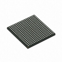
XC6SLX45-2CSG324I Xilinx Inc, XC6SLX45-2CSG324I Datasheet - Page 44

XC6SLX45-2CSG324I
Manufacturer Part Number
XC6SLX45-2CSG324I
Description
FPGA Spartan®-6 Family 43661 Cells 45nm (CMOS) Technology 1.2V 324-Pin CSBGA
Manufacturer
Xilinx Inc
Series
Spartan® 6 LXr
Specifications of XC6SLX45-2CSG324I
Package
324CSBGA
Family Name
Spartan®-6
Device Logic Cells
43661
Device Logic Units
27288
Number Of Registers
54576
Typical Operating Supply Voltage
1.2 V
Maximum Number Of User I/os
218
Ram Bits
2138112
Number Of Logic Elements/cells
43661
Number Of Labs/clbs
3411
Total Ram Bits
2138112
Number Of I /o
218
Voltage - Supply
1.14 V ~ 1.26 V
Mounting Type
Surface Mount
Operating Temperature
-40°C ~ 100°C
Package / Case
324-LFBGA, CSPBGA
No. Of Logic Blocks
6822
No. Of Macrocells
43661
Family Type
Spartan-6
No. Of Speed Grades
2
No. Of I/o's
218
Clock Management
DCM, PLL
Core Supply Voltage Range
1.14V
Rohs Compliant
Yes
Lead Free Status / RoHS Status
Lead free / RoHS Compliant
Number Of Gates
-
Lead Free Status / RoHS Status
Lead free / RoHS Compliant
Available stocks
Company
Part Number
Manufacturer
Quantity
Price
Company:
Part Number:
XC6SLX45-2CSG324I
Manufacturer:
XILINX
Quantity:
230
Company:
Part Number:
XC6SLX45-2CSG324I
Manufacturer:
XILINX33
Quantity:
586
Company:
Part Number:
XC6SLX45-2CSG324I
Manufacturer:
Xilinx Inc
Quantity:
10 000
Table 43: DSP48A1 Switching Characteristics (Cont’d)
DS162 (v2.0) March 31, 2011
Preliminary Product Specification
Notes:
1.
2.
Clock to Out from Output Register Clock to Output Pin
T
Clock to Out from Pipeline Register Clock to Output Pins
T
Clock to Out from Input Register Clock to Output Pins
T
T
T
T
Combinatorial Delays from Input Pins to Output Pins
T
T
T
T
T
Maximum Frequency
F
DSPCKO_P_PREG
DSPCKO_P_MREG
DSPCKO_P_A1REG
DSPCKO_P_B1REG
DSPCKO_P_CREG
DSPCKO_P_DREG
DSPDO_A_P
DSPDO_B_P
DSPDO_C_P
DSPDO_D_P
DSPDO_OPMODE_P
MAX
A Yes signifies that the component is in the path. A No signifies that the component is being bypassed. N/A signifies not applicable because
no path exists.
Implemented in the post-adder by adding to zero.
Symbol
CLK (PREG) to P output
CLK (MREG) to P output
CLK (A1REG) to P output
CLK (B1REG) to P output
CLK (CREG) to P output
CLK (DREG) to P output
A input to P output
B input to P output
C input to P output
D input to P output
OPMODE input to P output
All registers used
Description
www.xilinx.com
Spartan-6 FPGA Data Sheet: DC and Switching Characteristics
adder
Pre-
N/A
N/A
N/A
N/A
N/A
N/A
N/A
N/A
N/A
Yes
Yes
Yes
Yes
Yes
Yes
Yes
No
No
Multiplier
N/A
N/A
N/A
N/A
Yes
Yes
Yes
Yes
Yes
Yes
Yes
Yes
Yes
Yes
Yes
No
No
No
adder
Post-
No
No
No
N/A
Yes
Yes
Yes
Yes
Yes
Yes
Yes
Yes
Yes
Yes
Yes
Yes
Yes
Yes
(2)
(2)
(2)
1.20
3.38
5.02
5.02
3.12
6.77
2.85
3.35
4.56
3.22
6.01
6.27
2.69
6.31
6.43
4.84
3.11
390
-3
Speed Grade
3.95
1.34
5.87
5.87
3.64
7.92
3.33
3.93
5.22
3.76
6.54
7.34
3.15
7.38
7.52
5.66
3.49
333
-3N
1.34
3.95
5.87
5.87
3.64
7.92
3.33
3.93
5.22
3.76
6.54
7.34
3.15
7.38
7.52
5.66
3.49
333
-2
12.53
11.96
11.81
11.84
1.90
5.83
9.65
9.63
5.24
4.73
6.74
8.94
5.55
9.76
4.68
9.25
5.03
213
-1L
Units
MHz
ns
ns
ns
ns
ns
ns
ns
ns
ns
ns
ns
ns
ns
ns
ns
ns
ns
44


