NSB1706DMW5T1G ON Semiconductor, NSB1706DMW5T1G Datasheet
NSB1706DMW5T1G
Manufacturer Part Number
NSB1706DMW5T1G
Description
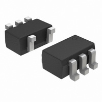
TRANS BRT NPN DUAL 50V SOT353
Manufacturer
ON Semiconductor
Datasheet
1.NSB1706DMW5T1G.pdf
(3 pages)
Specifications of NSB1706DMW5T1G
Transistor Type
2 NPN - Pre-Biased (Dual)
Current - Collector (ic) (max)
100mA
Voltage - Collector Emitter Breakdown (max)
50V
Resistor - Base (r1) (ohms)
4.7K
Resistor - Emitter Base (r2) (ohms)
47K
Dc Current Gain (hfe) (min) @ Ic, Vce
80 @ 5mA, 10V
Vce Saturation (max) @ Ib, Ic
250mV @ 1mA, 10mA
Current - Collector Cutoff (max)
500nA
Power - Max
250mW
Mounting Type
Surface Mount
Package / Case
SC-70-5, SC-88A, SOT-323-5, SOT-353, 5-TSSOP
Lead Free Status / RoHS Status
Lead free / RoHS Compliant
Frequency - Transition
-
Other names
NSB1706DMW5T1GOS
Available stocks
Company
Part Number
Manufacturer
Quantity
Price
Company:

Part Number:
NSB1706DMW5T1G
Manufacturer:
ON
Quantity:
39 000
Company:
Part Number:
NSB1706DMW5T1G
Manufacturer:
ON
Quantity:
30 000


NSB1706DMW5T1G
Dual Bias Resistor
Transistor
NPN Silicon Surface Mount Transistors
with Monolithic Bias Resistor Network
a monolithic bias network consisting of two resistors; a series base
resistor and a base−emitter resistor. These digital transistors are
designed to replace a single device and its external resistor bias
network. The BRT eliminates these individual components by
integrating them into a single device. In the NSB1706DMW5T1G,
two BRT devices are housed in the SC−88A package which is ideal for
low power surface mount applications where board space is at a
premium.
Features
•
•
•
•
Stresses exceeding Maximum Ratings may damage the device. Maximum
Ratings are stress ratings only. Functional operation above the Recommended
Operating Conditions is not implied. Extended exposure to stresses above the
Recommended Operating Conditions may affect device reliability.
1. FR−4 @ Minimum Pad.
2. FR−4 @ 1.0 x 1.0 inch Pad.
MAXIMUM RATINGS
(T
THERMAL CHARACTERISTICS
© Semiconductor Components Industries, LLC, 2009
October, 2009 − Rev. 4
Collector-Base Voltage
Collector-Emitter Voltage
Collector Current
Total Device Dissipation
T
Derate above 25°C
Thermal Resistance, Junction-to-Ambient
Total Device Dissipation
T
Derate above 25°C
Thermal Resistance, Junction-to-Ambient
Thermal Resistance, Junction-to-Lead
Junction and Storage Temperature
A
The Bias Resistor Transistor (BRT) contains a single transistor with
A
A
Compliant
Simplifies Circuit Design
Reduces Board Space
Reduces Component Count
These Devices are Pb−Free, Halogen Free/BFR Free and are RoHS
= 25°C unless otherwise noted, common for Q
= 25°C
= 25°C
(Both Junctions Heated)
(One Junction Heated)
Characteristic
Characteristic
Rating
Symbol
Symbol
Symbol
T
V
V
R
R
R
J
P
P
CBO
CEO
, T
I
qJA
qJA
qJL
C
D
D
stg
1
and Q
187 (Note 1)
256 (Note 2)
670 (Note 1)
490 (Note 2)
250 (Note 1)
385 (Note 2)
493 (Note 1)
325 (Note 2)
188 (Note 1)
208 (Note 2)
−55 to +150
1.5 (Note 1)
2.0 (Note 2)
2.0 (Note 1)
3.0 (Note 2)
Value
2
Max
Max
)
100
50
50
1
mW/°C
mW/°C
mAdc
°C/W
°C/W
°C/W
Unit
Unit
Unit
mW
mW
Vdc
Vdc
°C
†For information on tape and reel specifications,
NSB1706DMW5T1G
including part orientation and tape sizes, please
refer to our Tape and Reel Packaging Specification
Brochure, BRD8011/D.
(Note: Microdot may be in either location)
Device
R1
ORDERING INFORMATION
(1)
MARKING DIAGRAM
U6 = Device Marking
M = Date Code
G
http://onsemi.com
R2
= Pb−Free Package
1
(5)
Q1
Q1
CASE 419A
STYLE 1
SC−88A
U6 M G
(Pb−Free)
Package
SC−88A
1
(2)
Publication Order Number:
G
Q2
(4)
NSB1706DMW5T1/D
R2
Tape & Reel
Shipping
(3)
3000 /
R1
†
Related parts for NSB1706DMW5T1G
Image
Part Number
Description
Manufacturer
Datasheet
Request
R

Part Number:
Description:
ON Semiconductor [VOLTAGE REGULATOR]
Manufacturer:
ON Semiconductor
Datasheet:
Part Number:
Description:
357-036-542-201 CARDEDGE 36POS DL .156 BLK LOPRO
Manufacturer:
ON Semiconductor
Datasheet:
Part Number:
Description:
357-036-542-201 CARDEDGE 36POS DL .156 BLK LOPRO
Manufacturer:
ON Semiconductor
Datasheet:
Part Number:
Description:
357-036-542-201 CARDEDGE 36POS DL .156 BLK LOPRO
Manufacturer:
ON Semiconductor
Datasheet:
Part Number:
Description:
357-036-542-201 CARDEDGE 36POS DL .156 BLK LOPRO
Manufacturer:
ON Semiconductor
Datasheet:
Part Number:
Description:
357-036-542-201 CARDEDGE 36POS DL .156 BLK LOPRO
Manufacturer:
ON Semiconductor
Datasheet:
Part Number:
Description:
357-036-542-201 CARDEDGE 36POS DL .156 BLK LOPRO
Manufacturer:
ON Semiconductor
Datasheet:
Part Number:
Description:
357-036-542-201 CARDEDGE 36POS DL .156 BLK LOPRO
Manufacturer:
ON Semiconductor
Datasheet:
Part Number:
Description:
357-036-542-201 CARDEDGE 36POS DL .156 BLK LOPRO
Manufacturer:
ON Semiconductor
Datasheet:
Part Number:
Description:
357-036-542-201 CARDEDGE 36POS DL .156 BLK LOPRO
Manufacturer:
ON Semiconductor
Datasheet:
Part Number:
Description:
357-036-542-201 CARDEDGE 36POS DL .156 BLK LOPRO
Manufacturer:
ON Semiconductor
Datasheet:
Part Number:
Description:
Manufacturer:
ON Semiconductor
Datasheet:
Part Number:
Description:
Manufacturer:
ON Semiconductor
Datasheet:
Part Number:
Description:
Manufacturer:
ON Semiconductor
Datasheet:
NSB1706DMW5T1G Summary of contents
Page 1
... The BRT eliminates these individual components by integrating them into a single device. In the NSB1706DMW5T1G, two BRT devices are housed in the SC−88A package which is ideal for low power surface mount applications where board space premium ...
Page 2
ELECTRICAL CHARACTERISTICS Characteristic OFF CHARACTERISTICS Collector-Base Cutoff Current ( Collector-Emitter Cutoff Current ( Emitter-Base Cutoff Current ( ...
Page 3
... Pb−Free strategy and soldering details, please download the ON Semiconductor Soldering and Mounting Techniques Reference Manual, SOLDERRM/D. ON Semiconductor and are registered trademarks of Semiconductor Components Industries, LLC (SCILLC). SCILLC reserves the right to make changes without further notice to any products herein ...