Thermal Characteristics
Electrical Characteristics
Maximum Ratings
Features
•
•
•
•
•
Collector-Base Voltage
Collector-Emitter Voltage
Emitter-Base Voltage
Collector Current - Continuous (Note 1)
Power Dissipation (Note 1)
Thermal Resistance, Junction to Ambient (Note 1)
Operating and Storage and Temperature Range
OFF CHARACTERISTICS (Note 3)
Collector-Base Breakdown Voltage
Collector-Emitter Breakdown Voltage
Emitter-Base Breakdown Voltage
Collector Cutoff Current
Emitter Cutoff Current
ON CHARACTERISTICS (Note 3)
DC Current Gain
Collector-Emitter Saturation Voltage
Base-Emitter Saturation Voltage
SMALL SIGNAL CHARACTERISTICS
Output Capacitance
Input Capacitance
Small Signal Current Gain
Current Gain-Bandwidth Product
Notes:
MMBT4124
Document number: DS30105 Rev. 11 - 2
Epitaxial Planar Die Construction
Complementary PNP Type Available (MMBT4126)
Ideal for Medium Power Amplification and Switching
Lead, Halogen and Antimony Free, RoHS Compliant
"Green" Device (Notes 2 and 4)
1. Device mounted on FR-4 PCB, 1 inch x 0.85 inch x 0.062 inch; pad layout as shown on Diodes Inc. suggested pad layout document AP02001, which
2. No purposefully added lead. Halogen and Antimony Free.
3. Short duration pulse test used to minimize self-heating effect.
4. Product manufactured with Data Code V9 (week 33, 2008) and newer are built with Green Molding Compound. Product manufactured prior to Date
can be found on our website at http://www.diodes.com/datasheets/ap02001.pdf.
Code V9 are built with Non-Green Molding Compound and may contain Halogens or Sb
Characteristic
Characteristic
Characteristic
@T
A
= 25°C unless otherwise specified
@T
A
= 25°C unless otherwise specified
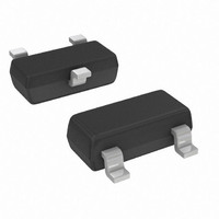
Top View
www.diodes.com
V
V
V
Symbol
V
V
(BR)CBO
(BR)CEO
(BR)EBO
CE(SAT)
BE(SAT)
I
C
I
C
h
CBO
EBO
1 of 3
h
f
obo
FE
ibo
fe
T
NPN SMALL SIGNAL SURFACE MOUNT TRANSISTOR
Mechanical Data
•
•
•
•
•
•
•
•
T
Symbol
Symbol
Device Schematic
B
J
V
V
V
R
, T
P
CBO
CEO
EBO
I
θ JA
C
Please click here to visit our online spice models database.
D
Min
120
120
300
5.0
STG
Case: SOT-23
Case Material: Molded Plastic, “Green” Molding Compound,
Note 4. UL Flammability Classification Rating 94V-0
Moisture Sensitivity: Level 1 per J-STD-020D
Terminal Connections: See Diagram
Terminals: Matte Tin Finish annealed over Alloy 42 leadframe
(Lead Free Plating) Solderable per MIL-STD-202, Method 208
Marking Information: See Page 3
Ordering Information: See Page 3
Weight: 0.008 grams (approximate)
30
25
60
⎯
⎯
⎯
⎯
⎯
⎯
C
E
2
Max
0.30
0.95
O
360
480
4.0
8.0
50
50
⎯
⎯
⎯
⎯
⎯
3
Fire Retardants.
Unit
MHz
-55 to +150
nA
nA
pF
pF
⎯
⎯
V
V
V
V
V
Value
Value
200
300
417
5.0
30
25
I
I
I
V
V
I
I
I
I
V
V
V
f = 1.0kHz
V
f = 100MHz
C
C
E
C
C
C
C
CB
EB
CB
EB
CE
CE
= 10μA, I
= 10μA, I
= 1.0mA, I
= 2.0mA, V
= 50mA, V
= 50mA, I
= 50mA, I
= 20V, I
= 3.0V, I
= 1.0V, I
= 5.0V, f = 1.0MHz, I
= 0.5V, f = 1.0MHz, I
= 20V, I
Test Condition
C
E
E
B
B
C
C
B
C
= 0
= 0
CE
CE
= 0V
= 5.0mA
= 5.0mA
= 10mA,
= 0
= 0V
= 2.0mA,
= 1.0V
= 1.0V
MMBT4124
© Diodes Incorporated
°C/W
Unit
Unit
mW
mA
°C
V
V
V
January 2009
C
E
= 0
= 0