Mechanical Data
Electrical Characteristics
Features
Maximum Ratings
Collector-Base Voltage
Collector-Emitter Voltage
Emitter-Base Voltage
Collector Current
Power Dissipation
Thermal Resistance, Junction to Ambient
Operating and Storage Temperature Range
Collector-Base Breakdown Voltage
Collector-Emitter Breakdown Voltage
Emitter-Base Breakdown Voltage
DC Current Gain
Collector-Emitter Saturation Voltage
Base-Emitter Saturation Voltage
Base-Emitter Voltage
Collector-Cutoff Current
Gain Bandwidth Product
Output Capacitance
Noise Figure
•
•
•
•
•
•
•
•
•
•
•
•
•
•
•
Notes:
DS30275 Rev. 9 - 2
Epitaxial Die Construction
Complementary NPN Types Available (BC847AT,BT,CT)
Ultra-Small Surface Mount Package
Lead Free/RoHS Compliant (Note 2)
Qualified to AEC-Q101 Standards for High Reliability
"Green" Device (Note 4 and 5)
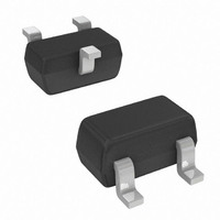
Case: SOT-523
Case Material - Molded Plastic. UL Flammability
Classification Rating 94V-0
Moisture Sensitivity: Level 1 per J-STD-020C
Terminals: Solderable per MIL-STD-202, Method 208
Lead Free Plating (Matte Tin Finish annealed over Alloy
42 leadframe).
Terminal Connections: See Diagram
Marking Code: See Table Below & Diagram on Page 2
Ordering & Date Code Information: See Page 2
Weight: 0.002 grams (approximate)
1. Device mounted on FR-4 PCB, 1 inch x 0.85 inch x 0.062 inch; pad layout as shown on Diodes Inc. suggested pad layout document AP02001, which
2. No purposefully added lead
3. Short duration pulse test used to minimize self-heating effect.
4. Diodes Inc.'s "Green" policy can be found on our website at http://www.diodes.com/products/lead_free/index.php.
5. Product manufactured with Date Code UO (week 40, 2007) and newer are built with Green Molding Compound. Product manufactured prior to Date
Code UO are built with Non-Green Molding Compound and may contain Halogens or Sb2O3 Fire Retardants.
can be found on our website at http://www.diodes.com/datasheets/ap02001.pdf.
Characteristic
Characteristic
(Note 3) Current Gain
@T
A
= 25°C unless otherwise specified
@T
A
= 25°C unless otherwise specified
(Note 3)
(Note 3)
(Note 3)
(Note 3)
(Note 3)
(Note 3)
(Note 3)
A
B
C
(Note 1)
(Note 1)
V
V
V
V
Symbol
V
V
(BR)CBO
(BR)CEO
(BR)EBO
CE(SAT)
BE(SAT)
BE(ON)
I
C
h
CBO
NF
f
FE
OB
T
www.diodes.com
K
J
BC857AT
BC857BT
BC857CT
1 of 3
B
Type
-600
Min
125
220
420
100
-50
-45
—
—
—
—
—
—
—
—
-5
PNP SMALL SIGNAL SURFACE MOUNT TRANSISTOR
TOP VIEW
Symbol
T
V
V
V
j
R
, T
G
H
A
P
CBO
CEO
EBO
I
θ JA
C
d
STG
D
C
-700
-900
Typ
290
520
—
—
—
—
—
—
—
—
—
—
—
—
—
E
B C
Marking
N
-300
-650
-750
-820
Max
250
475
800
-4.0
-15
4.5
10
—
—
—
—
—
—
3W
3G
3V
L
BC857AT, BT, CT
MHz
Unit
mV
mV
mV
NA
µA
pF
dB
—
-55 to +150
V
V
V
Value
-100
-5.0
150
833
-50
-45
I
I
I
V
I
I
I
I
V
V
V
V
V
V
I
R
BW = 200Hz
M
C
C
E
C
C
C
C
C
CE
CE
CE
CB
CB
CE
CB
S
= 10μA, I
= 10mA, I
= 1μA, I
= -10mA, I
= -100mA, I
= -10mA, I
= -100mA, I
= -0.2mA, V
= 2.0KΩ, f = 1.0KHz,
= -5.0V, I
= -5.0V, I
= -5.0V, I
= -30V
= -30V, T
= -5.0V, I
= -10V, f = 1.0MHz
Dim
C
All Dimensi
G
M
Test Condition
A
B
C
D
H
K
N
α
J
L
B
= 0
B
B
B
= 0
C
C
C
A
C
= 0
B
B
CE
= -0.5mA
= -0.5mA
= -2.0mA
= -2.0mA
= -10mA
= 150°C
= -10mA, f = 100MHz
= -5.0mA
= -5.0mA
0.15
0.75
1.45
0.90
1.50
0.00
0.60
0.10
0.10
0.45
Min
= -5.0Vdc,
SOT-523
⎯
0°
BC857AT, BT, CT
© Diodes Incorporated
°C/W
ons in
Unit
mW
mA
Max
0.30
0.85
1.75
1.10
1.70
0.10
0.80
0.30
0.20
0.65
°C
V
V
V
⎯
8°
mm
0.22
0.80
1.60
0.50
1.00
1.60
0.05
0.75
0.22
0.12
0.50
Typ
⎯