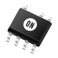
NCP1236AD65R2G ON Semiconductor, NCP1236AD65R2G Datasheet - Page 21

NCP1236AD65R2G
Manufacturer Part Number
NCP1236AD65R2G
Description
IC CTLR CURR MODE 65KHZ 7-SOIC
Manufacturer
ON Semiconductor
Datasheet
1.NCP1236AD65R2G.pdf
(34 pages)
Specifications of NCP1236AD65R2G
Frequency - Max
70kHz
Pwm Type
Current Mode
Number Of Outputs
1
Duty Cycle
85%
Voltage - Supply
9.5 V ~ 28 V
Buck
No
Boost
No
Flyback
Yes
Inverting
No
Doubler
No
Divider
No
Cuk
No
Isolated
Yes
Operating Temperature
-40°C ~ 125°C
Package / Case
8-SOIC (0.154", 3.90mm Width) 7 leads
Duty Cycle (max)
85 %
Output Current
500 mA
Mounting Style
SMD/SMT
Switching Frequency
65 KHz
Operating Supply Voltage
- 0.3 V to + 28 V
Supply Current
+/- 30 mA
Maximum Operating Temperature
+ 125 C
Fall Time
40 ns
Minimum Operating Temperature
- 40 C
Rise Time
40 ns
Lead Free Status / RoHS Status
Lead free / RoHS Compliant
Available stocks
Company
Part Number
Manufacturer
Quantity
Price
Company:
Part Number:
NCP1236AD65R2G
Manufacturer:
ON Semiconductor
Quantity:
500
Part Number:
NCP1236AD65R2G
Manufacturer:
ON/安森美
Quantity:
20 000
protection, an offset proportional to the input voltage is
added on the CS signal by turning on an internal current
source: by adding an external resistor in series between the
sense resistor and the CS pin, a voltage offset is created
across it by the current. The compensation can be adjusted
by changing the value of the resistor.
sense signal is small, i.e. in light load conditions, where it
input, and its output is periodically sampled and reset, in
order to follow closely the input voltage variations. The
sample and reset events are given by the V
comparator used for sampling detection for the AC line
To compensate this and have an accurate overpower
But this offset is unwanted to appear when the current
A 3 bit A/D converter with the peak detector senses the ac
HV
FB
I
LIMIT
I
P
Figure 38. Line Compensation for True Overpower Protection
V
HVstop
Figure 39. Schematic Overpower Compensation Circuit
Peak Detector
Converter
V
A/D 3 bit
FB (OPC)
High
Line
+
t
delay
HV Timer
(68 ms)
HV(stop)
t
http://onsemi.com
hv
Register
3 bit
To CS
Block
21
would be in the same order of magnitude. Therefore the
compensation current is only added when the FB voltage is
higher than V
voltage, there is needed an additional circuitry to read or at
least closely estimate the actual voltage on the bulk
capacitor.
input. If only the DC high voltage input is used, no reset
signal is generated by the V
watch dog is used to generate the sampling events for
sampling the DC input high voltage line.
t
delay
However, because the HV pin can be connected to an ac
T
LEB
blanking
Low
Line
I ctrl
I Generator
S
R
Q
Q
FB(OPCE)
Brown Out
time
compensated
CS
Watch
(32 ms)
.
Dog
I
P
to be
HV(stop)
condition and the 32 ms


