BSS63LT1G ON Semiconductor, BSS63LT1G Datasheet

TRANS PNP 100V 100MA SOT-23

BSS63LT1G

Manufacturer Part Number
BSS63LT1G
Description
TRANS PNP 100V 100MA SOT-23
Manufacturer
ON Semiconductor
Datasheet

Specifications of BSS63LT1G

Transistor Type
PNP
Current - Collector (ic) (max)
100mA
Voltage - Collector Emitter Breakdown (max)
100V
Vce Saturation (max) @ Ib, Ic
250mV @ 2.5mA, 25mA
Dc Current Gain (hfe) (min) @ Ic, Vce
30 @ 25mA, 1V
Power - Max
225mW
Frequency - Transition
95MHz
Mounting Type
Surface Mount
Package / Case
SOT-23-3, TO-236-3, Micro3™, SSD3, SST3
Transistor Polarity
PNP
Number Of Elements
1
Collector-emitter Voltage
100V
Collector-base Voltage
110V
Emitter-base Voltage
6V
Collector Current (dc) (max)
100mA
Dc Current Gain (min)
30
Power Dissipation
300mW
Frequency (max)
95MHz
Operating Temp Range
-55C to 150C
Operating Temperature Classification
Military
Mounting
Surface Mount
Pin Count
3
Package Type
SOT-23
Configuration
Single
Mounting Style
SMD/SMT
Collector- Emitter Voltage Vceo Max
100 V
Emitter- Base Voltage Vebo
6 V
Continuous Collector Current
- 0.1 A
Maximum Dc Collector Current
0.1 A
Maximum Operating Frequency
95 MHz
Maximum Operating Temperature
+ 150 C
Dc Collector/base Gain Hfe Min
30 at 10 mA at 1 V
Minimum Operating Temperature
- 55 C
Lead Free Status / RoHS Status
Lead free / RoHS Compliant
Current - Collector Cutoff (max)
-
Lead Free Status / Rohs Status
Compliant
Other names
BSS63LT1G
BSS63LT1GOSTR

Available stocks

Company
Part Number
Manufacturer
Quantity
Price
Part Number:
BSS63LT1G
Manufacturer:
ON Semiconductor
Quantity:
16 850
Part Number:
BSS63LT1G
Manufacturer:
ON
Quantity:
30 000
Part Number:
BSS63LT1G
Manufacturer:
ON/安森美
Quantity:
20 000
Company:
Part Number:
BSS63LT1G
Quantity:
17 990
Company:
Part Number:
BSS63LT1G
Quantity:
17 685
Company:
Part Number:
BSS63LT1G
Quantity:
24 000
BSS63LT1G
High Voltage Transistor
PNP Silicon
Features
Stresses exceeding Maximum Ratings may damage the device. Maximum
Ratings are stress ratings only. Functional operation above the Recommended
Operating Conditions is not implied. Extended exposure to stresses above the
Recommended Operating Conditions may affect device reliability.
1. FR−5 = 1.0 x 0.75 x 0.062 in.
2. Alumina = 0.4 x 0.3 x 0.024 in. 99.5% alumina.
© Semiconductor Components Industries, LLC, 2009
August, 2009 − Rev. 5
MAXIMUM RATINGS
THERMAL CHARACTERISTICS
Collector −Emitter Voltage
R
Collector Current − Continuous
Total Device Dissipation FR−5 Board,
(Note 1) T
Derate above 25°C
Thermal Resistance Junction−to−Ambient
Total Device Dissipation
Alumina Substrate, (Note 2)
T
Derate above 25°C
Thermal Resistance, Junction−to−Ambient
Junction and Storage Temperature
A
Compliant
These Devices are Pb−Free, Halogen Free/BFR Free and are RoHS
BE
= 25°C
= 10 kW
A
= 25°C
Characteristic
Rating
Symbol
Symbol
T
V
V
R
R
J
P
P
CEO
, T
CER
I
qJA
qJA
C
D
D
stg
−55 to
Value
+150
−100
−110
−100
Max
225
556
300
417
1.8
2.4
1
mW/°C
mW/°C
mAdc
°C/W
°C/W
Unit
Unit
mW
mW
Vdc
Vdc
°C
†For information on tape and reel specifications,
BSS63LT1G
including part orientation and tape sizes, please
refer to our Tape and Reel Packaging Specifications
Brochure, BRD8011/D.
*Date Code orientation and/or overbar may
Device
vary depending upon manufacturing location.
(Note: Microdot may be in either location)
ORDERING INFORMATION
BM
M
G
MARKING DIAGRAM
http://onsemi.com
BASE
1
(Pb−free)
Package
= Device Code
= Date Code*
= Pb−Free Package
SOT−23
1
CASE 318
STYLE 6
SOT−23
BM M G
COLLECTOR
Publication Order Number:
2
G
EMITTER
3
2
3
3000/Tape & Reel
Shipping
BSS63LT1/D

Related parts for BSS63LT1G

BSS63LT1G Summary of contents

Page 1

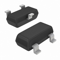
... D 300 mW/°C 2.4 R 417 °C/W qJA −55 to °C J stg +150 BSS63LT1G †For information on tape and reel specifications, including part orientation and tape sizes, please refer to our Tape and Reel Packaging Specifications Brochure, BRD8011/D. 1 http://onsemi.com COLLECTOR 3 1 BASE 2 EMITTER SOT−23 ...

Page 2

ELECTRICAL CHARACTERISTICS Characteristic OFF CHARACTERISTICS Collector −Emitter Breakdown Voltage (I = −100 mAdc) C Collector −Emitter Breakdown Voltage (I = −10 mAdc kW Collector −Base Breakdown Voltage (I = −10 mAdc, ...

Page 3

... A A1 *For additional information on our Pb−Free strategy and soldering details, please download the ON Semiconductor Soldering and Mounting Techniques Reference Manual, SOLDERRM/D. ON Semiconductor and are registered trademarks of Semiconductor Components Industries, LLC (SCILLC). SCILLC reserves the right to make changes without further notice to any products herein. SCILLC makes no warranty, representation or guarantee regarding the suitability of its products for any particular purpose, nor does SCILLC assume any liability arising out of the application or use of any product or circuit, and specifically disclaims any and all liability, including without limitation special, consequential or incidental damages. “ ...

Related keywords