2N3904RLRAG ON Semiconductor, 2N3904RLRAG Datasheet - Page 4
2N3904RLRAG
Manufacturer Part Number
2N3904RLRAG
Description
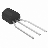
TRANS NPN GP 200MA 40V TO92
Manufacturer
ON Semiconductor
Type
General Purposer
Specifications of 2N3904RLRAG
Transistor Type
NPN
Current - Collector (ic) (max)
200mA
Voltage - Collector Emitter Breakdown (max)
40V
Vce Saturation (max) @ Ib, Ic
300mV @ 5mA, 50mA
Dc Current Gain (hfe) (min) @ Ic, Vce
100 @ 10mA, 1V
Power - Max
625mW
Frequency - Transition
300MHz
Mounting Type
Through Hole
Package / Case
TO-92-3 (Standard Body), TO-226
Configuration
Single
Transistor Polarity
NPN
Mounting Style
Through Hole
Collector- Emitter Voltage Vceo Max
40 V
Emitter- Base Voltage Vebo
6 V
Continuous Collector Current
0.2 A
Maximum Dc Collector Current
0.2 A
Power Dissipation
625 mW
Maximum Operating Frequency
300 MHz
Maximum Operating Temperature
+ 150 C
Dc Collector/base Gain Hfe Min
40 at 0.1 mA at 1 V
Minimum Operating Temperature
- 55 C
Current, Collector
200 mA
Current, Gain
30
Frequency
300 MHz
Package Type
TO-92
Polarity
NPN
Primary Type
Si
Resistance, Thermal, Junction To Case
83.3 °C/W
Voltage, Breakdown, Collector To Emitter
40 V
Voltage, Collector To Base
60 V
Voltage, Collector To Emitter
40 V
Voltage, Collector To Emitter, Saturation
0.3 V
Voltage, Emitter To Base
6 V
Number Of Elements
1
Collector-emitter Voltage
40V
Collector-base Voltage
60V
Emitter-base Voltage
6V
Collector Current (dc) (max)
200mA
Frequency (max)
300MHz
Operating Temp Range
-55C to 150C
Operating Temperature Classification
Military
Mounting
Through Hole
Pin Count
3
Dc
N/A
Lead Free Status / RoHS Status
Lead free / RoHS Compliant
Current - Collector Cutoff (max)
-
Lead Free Status / Rohs Status
Lead free / RoHS Compliant
Other names
2N3904RLRAGOSTR
Available stocks
Company
Part Number
Manufacturer
Quantity
Price
Company:

Part Number:
2N3904RLRAG
Manufacturer:
ON
Quantity:
244 000
Company:
Part Number:
2N3904RLRAG
Manufacturer:
ON
Quantity:
4 000


2N3903, 2N3904
+3 V
DUTY CYCLE = 2%
300 ns
+10.9 V
275
10 k
- 0.5 V
C
< 4 pF*
< 1 ns
S
* Total shunt capacitance of test jig and connectors
Figure 1. Delay and Rise Time Equivalent Test Circuit
+3 V
< 500 ms
t
10 < t
1
1
+10.9 V
DUTY CYCLE = 2%
275
10 k
0
C
< 4 pF*
1N916
S
- 9.1 V′
< 1 ns
* Total shunt capacitance of test jig and connectors
Figure 2. Storage and Fall Time Equivalent Test Circuit
http://onsemi.com
4
Related parts for 2N3904RLRAG
Image
Part Number
Description
Manufacturer
Datasheet
Request
R

Part Number:
Description:
ON Semiconductor [VOLTAGE REGULATOR]
Manufacturer:
ON Semiconductor
Datasheet:
Part Number:
Description:
357-036-542-201 CARDEDGE 36POS DL .156 BLK LOPRO
Manufacturer:
ON Semiconductor
Datasheet:
Part Number:
Description:
357-036-542-201 CARDEDGE 36POS DL .156 BLK LOPRO
Manufacturer:
ON Semiconductor
Datasheet:
Part Number:
Description:
357-036-542-201 CARDEDGE 36POS DL .156 BLK LOPRO
Manufacturer:
ON Semiconductor
Datasheet:
Part Number:
Description:
357-036-542-201 CARDEDGE 36POS DL .156 BLK LOPRO
Manufacturer:
ON Semiconductor
Datasheet:
Part Number:
Description:
357-036-542-201 CARDEDGE 36POS DL .156 BLK LOPRO
Manufacturer:
ON Semiconductor
Datasheet:
Part Number:
Description:
357-036-542-201 CARDEDGE 36POS DL .156 BLK LOPRO
Manufacturer:
ON Semiconductor
Datasheet:
Part Number:
Description:
357-036-542-201 CARDEDGE 36POS DL .156 BLK LOPRO
Manufacturer:
ON Semiconductor
Datasheet:
Part Number:
Description:
357-036-542-201 CARDEDGE 36POS DL .156 BLK LOPRO
Manufacturer:
ON Semiconductor
Datasheet:
Part Number:
Description:
357-036-542-201 CARDEDGE 36POS DL .156 BLK LOPRO
Manufacturer:
ON Semiconductor
Datasheet:
Part Number:
Description:
357-036-542-201 CARDEDGE 36POS DL .156 BLK LOPRO
Manufacturer:
ON Semiconductor
Datasheet:
Part Number:
Description:
Manufacturer:
ON Semiconductor
Datasheet:
Part Number:
Description:
Manufacturer:
ON Semiconductor
Datasheet:
Part Number:
Description:
Manufacturer:
ON Semiconductor
Datasheet: