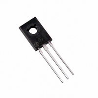
MJE181G ON Semiconductor, MJE181G Datasheet - Page 4

MJE181G
Manufacturer Part Number
MJE181G
Description
TRANS POWER NPN 3A 60V TO225AA
Manufacturer
ON Semiconductor
Type
Powerr
Specifications of MJE181G
Transistor Type
NPN
Current - Collector (ic) (max)
3A
Voltage - Collector Emitter Breakdown (max)
60V
Vce Saturation (max) @ Ib, Ic
1.7V @ 600mA, 3A
Dc Current Gain (hfe) (min) @ Ic, Vce
50 @ 100mA, 1V
Power - Max
12.5W
Frequency - Transition
50MHz
Mounting Type
Through Hole
Package / Case
TO-225-3
Current, Collector
3 A
Current, Gain
12
Frequency
50 MHz
Package Type
TO-225AA
Polarity
NPN
Power Dissipation
1.5 W
Primary Type
Si
Resistance, Thermal, Junction To Case
10 °C/W
Voltage, Breakdown, Collector To Emitter
60 V
Voltage, Collector To Base
60 V
Voltage, Collector To Emitter
60 V
Voltage, Collector To Emitter, Saturation
1.7 V
Voltage, Emitter To Base
7 V
Lead Free Status / RoHS Status
Lead free / RoHS Compliant
Current - Collector Cutoff (max)
-
Lead Free Status / Rohs Status
RoHS Compliant part
Electrostatic Device
Other names
MJE181GOS
Available stocks
Company
Part Number
Manufacturer
Quantity
Price
Company:
Part Number:
MJE181G
Manufacturer:
ON Semiconductor
Quantity:
900
a transistor − average junction temperature and second
breakdown. Safe operating area curves indicate I
limits of the transistor that must be observed for reliable
operation; i.e., the transistor must not be subjected to greater
dissipation than the curves indicate.
10K
There are two limitations on the power handling ability of
0.05
0.02
0.01
500
300
200
100
5.0
2.0
1.0
0.5
0.2
0.1
5K
3K
2K
1K
50
30
20
10
10
0.01
1.0
NPN MJE181/182
PNP MJE171/172
0.02
V
2.0
t
f
CE
0.03 0.05
MJE170, MJE171, MJE172 (PNP), MJE180, MJE181, MJE182 (NPN)
BONDING WIRE LIMITED
THERMALLY LIMITED @
SECOND BREAKDOWN LIMITED
CURVES APPLY BELOW
, COLLECTOR−EMITTER VOLTAGE (VOLTS)
T
T
RATED V
3.0
Figure 5. MJE171, MJE172
J
C
I
C
Figure 7. Turn−Off Time
= 150°C
= 25°C (SINGLE PULSE)
, COLLECTOR CURRENT (AMPS)
5.0
CEO
0.1
dc
0.2
10
0.3
t
s
ACTIVE−REGION SAFE OPERATING AREA
0.5
5.0 ms
20
MJE171
MJE172
100 ms
30
1
V
I
I
T
C
B1
J
CC
/I
2
= 25°C
B
= I
= 30 V
= 10
50
B2
C
3
500 ms
http://onsemi.com
− V
CE
100
5
4
10
is variable depending on conditions. Second breakdown
pulse limits are valid for duty cycles to 10% provided
T
Figure 4. At high case temperature, thermal limitations will
reduce the power that can be handled to values less than the
limitations imposed by second breakdown.
100
0.05
0.02
0.01
J(pk)
20
70
50
30
10
5.0
2.0
1.0
0.5
0.2
0.1
The data of Figures 5 and 6 is based on T
10
1.0
0.5 0.7
t 150°C. T
2.0
V
1.0
CE
, COLLECTOR−EMITTER VOLTAGE (VOLTS)
BONDING WIRE LIMITED
THERMALLY LIMITED @
SECOND BREAKDOWN LIMITED
CURVES APPLY BELOW
T
3.0
Figure 6. MJE181, MJE182
T
RATED V
J
V
C
= 150°C
R
Figure 8. Capacitance
= 25°C (SINGLE PULSE)
J(pk)
2.0
5.0 ms
, REVERSE VOLTAGE (VOLTS)
5.0
CEO
3.0
may be calculated from the data in
7.0
5.0
10
dc
7.0
C
ib
20
MJE181
MJE182
10
PNP MJE171/MJE172
NPN MJE181/MJE182
100 ms
C
J(pk)
30
ob
T
20
J
= 150°C; T
= 25°C
500 ms
50
30
70
100
50
C


