MJF122G ON Semiconductor, MJF122G Datasheet - Page 2
MJF122G
Manufacturer Part Number
MJF122G
Description
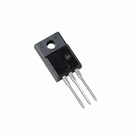
TRANS DARL NPN 5A 100V TO220FP
Manufacturer
ON Semiconductor
Datasheet
1.MJF122G.pdf
(7 pages)
Specifications of MJF122G
Transistor Type
NPN - Darlington
Current - Collector (ic) (max)
5A
Voltage - Collector Emitter Breakdown (max)
100V
Vce Saturation (max) @ Ib, Ic
3.5V @ 20mA, 5A
Current - Collector Cutoff (max)
10µA
Dc Current Gain (hfe) (min) @ Ic, Vce
2000 @ 3A, 3V
Power - Max
2W
Mounting Type
Through Hole
Package / Case
TO-220-3 Full Pack (Straight Leads)
Configuration
Single
Transistor Polarity
NPN
Mounting Style
Through Hole
Collector- Emitter Voltage Vceo Max
100 V
Emitter- Base Voltage Vebo
5 V
Collector- Base Voltage Vcbo
100 V
Maximum Dc Collector Current
5 A
Maximum Collector Cut-off Current
10 uA
Power Dissipation
30 W
Maximum Operating Temperature
+ 150 C
Continuous Collector Current
5 A
Dc Collector/base Gain Hfe Min
1000
Minimum Operating Temperature
- 65 C
Lead Free Status / RoHS Status
Lead free / RoHS Compliant
Frequency - Transition
-
Lead Free Status / Rohs Status
Lead free / RoHS Compliant
Other names
MJF122GOS
Available stocks
Company
Part Number
Manufacturer
Quantity
Price

Part Number:
MJF122G
Manufacturer:
ON/安森美
Quantity:
20 000


Î Î Î Î Î Î Î Î Î Î Î Î Î Î Î Î Î Î Î Î Î Î Î Î Î Î Î Î Î Î Î Î Î
Î Î Î Î Î Î Î Î Î Î Î Î Î Î Î Î Î Î Î Î Î Î Î Î Î Î Î Î Î Î Î Î Î
Î Î Î Î Î Î Î Î Î Î Î Î Î Î Î Î Î Î Î Î Î Î Î
Î Î Î Î Î Î Î Î Î Î Î Î Î Î Î Î Î Î Î Î Î Î Î
Î Î Î Î Î Î Î Î Î Î Î Î Î Î Î Î Î Î Î Î Î Î Î Î Î Î Î Î Î Î Î Î Î
Î Î Î Î Î Î Î Î Î Î Î Î Î Î Î Î Î Î Î Î Î Î Î Î Î Î Î Î Î Î Î Î Î
Î Î Î Î Î Î Î Î Î Î Î Î Î Î Î Î Î Î Î Î Î Î Î
Î Î Î Î Î Î Î Î Î Î Î Î Î Î Î Î Î Î Î Î Î Î Î
Î Î Î Î Î Î Î Î Î Î Î Î Î Î Î Î Î Î Î Î Î Î Î
Î Î Î Î Î Î Î Î Î Î Î Î Î Î Î Î Î Î Î Î Î Î Î
Î Î Î Î Î Î Î Î Î Î Î Î Î Î Î Î Î Î Î Î Î Î Î
Î Î Î Î Î Î Î Î Î Î Î Î Î Î Î Î Î Î Î Î Î Î Î
Î Î Î Î Î Î Î Î Î Î Î Î Î Î Î Î Î Î Î Î Î Î Î
Î Î Î Î Î Î Î Î Î Î Î Î Î Î Î Î Î Î Î Î Î Î Î
Î Î Î Î Î Î Î Î Î Î Î Î Î Î Î Î Î Î Î Î Î Î Î
Î Î Î Î Î Î Î Î Î Î Î Î Î Î Î Î Î Î Î Î Î Î Î
Î Î Î Î Î Î Î Î Î Î Î Î Î Î Î Î Î Î Î Î Î Î Î Î Î Î Î Î Î Î Î Î Î
Î Î Î Î Î Î Î Î Î Î Î Î Î Î Î Î Î Î Î Î Î Î Î Î Î Î Î Î Î Î Î Î Î
Î Î Î Î Î Î Î Î Î Î Î Î Î Î Î Î Î Î Î Î Î Î Î
Î Î Î Î Î Î Î Î Î Î Î Î Î Î Î Î Î Î Î Î Î Î Î
Î Î Î Î Î Î Î Î Î Î Î Î Î Î Î Î Î Î Î Î Î Î Î
Î Î Î Î Î Î Î Î Î Î Î Î Î Î Î Î Î Î Î Î Î Î Î
Î Î Î Î Î Î Î Î Î Î Î Î Î Î Î Î Î Î Î Î Î Î Î
Î Î Î Î Î Î Î Î Î Î Î Î Î Î Î Î Î Î Î Î Î Î Î
Î Î Î Î Î Î Î Î Î Î Î Î Î Î Î Î Î Î Î Î Î Î Î
Î Î Î Î Î Î Î Î Î Î Î Î Î Î Î Î Î Î Î Î Î Î Î Î Î Î Î Î Î Î Î Î Î
Î Î Î Î Î Î Î Î Î Î Î Î Î Î Î Î Î Î Î Î Î Î Î Î Î Î Î Î Î Î Î Î Î
Î Î Î Î Î Î Î Î Î Î Î Î Î Î Î Î Î Î Î Î Î Î Î
Î Î Î Î Î Î Î Î Î Î Î Î Î Î Î Î Î Î Î Î Î Î Î
Î Î Î Î Î Î Î Î Î Î Î Î Î Î Î Î Î Î Î Î Î Î Î
Î Î Î Î Î Î Î Î Î Î Î Î Î Î Î Î Î Î Î Î Î Î Î
Î Î Î Î Î Î Î Î Î Î Î Î Î Î Î Î Î Î Î Î Î Î Î
3. Pulse Test: Pulse Width v 300 ms, Duty Cycle v 2%.
ELECTRICAL CHARACTERISTICS
OFF CHARACTERISTICS
ON CHARACTERISTICS (Note 3)
DYNAMIC CHARACTERISTICS
R
D
APPROX.
APPROX.
1N5825 USED ABOVE I
MSD6100 USED BELOW I
B
1
Collector−Emitter Sustaining Voltage (Note 3)
Collector Cutoff Current
Collector Cutoff Current
Emitter Cutoff Current (V
DC Current Gain (I
DC Current Gain
Collector−Emitter Saturation Voltage (I
Collector−Emitter Saturation Voltage
Base−Emitter On Voltage (I
Small−Signal Current Gain (I
Output Capacitance
-12 V
, MUST BE FAST RECOVERY TYPES, e.g.,
+8 V
& R
V
V
(I
(V
(V
(V
2
1
C
C
0
t
DUTY CYCLE = 1%
r
CE
CB
CB
, t
VARIED TO OBTAIN DESIRED CURRENT LEVELS
= 100 mAdc, I
f
≤ 10 ns
= 50 Vdc, I
= 100 Vdc, I
= 10 Vdc, I
Figure 1. Switching Times Test Circuit
B
(I
≈ 100 mA
B
E
C
C
B
B
E
≈ 100 mA
= 0)
= 0, f = 0.1 MHz)
= 0.5 Adc, V
= 3 Adc, V
25 ms
= 0)
= 0)
FOR t
AND V
FOR NPN TEST CIRCUIT REVERSE ALL POLARITIES.
BE
C
= 5 Vdc, I
d
C
2
= 3 Adc, V
51
AND t
= 0
= 3 Adc, V
CE
CE
r
, D
= 3 Vdc)
R
D
B
Characteristic
1
= 3 Vdc)
+ 4 V
1
(I
C
IS DISCONNECTED
C
C
= 0)
CE
(T
= 3 Adc, I
= 5 Adc, I
CE
C
= 3 Vdc)
≈ 8 k
= 25_C unless otherwise noted)
= 4 Vdc, f = 1 MHz)
B
B
≈ 120
= 12 mAdc)
= 20 mAdc)
TUT
R
C
http://onsemi.com
- 30 V
V
CC
SCOPE
2
0.07
0.05
0.7
0.5
0.3
0.2
0.1
5
3
2
1
0.1
V
I
I
T
C
B1
CC
J
/I
= 25°C
MJF127
MJF122
B
= I
= 30 V
= 250
B2
0.2
Figure 2. Typical Switching Times
t
0.3
s
Î Î Î Î
Î Î Î Î
Î Î Î Î
Î Î Î Î
Î Î Î Î
Î Î Î Î
Î Î Î Î
Î Î Î Î
Î Î Î Î
Î Î Î Î
Î Î Î Î
Î Î Î Î
Î Î Î Î
Î Î Î Î
Î Î Î Î
Î Î Î Î
Î Î Î Î
Î Î Î Î
Î Î Î Î
Î Î Î Î
Î Î Î Î
Î Î Î Î
Î Î Î Î
Î Î Î Î
I
C
, COLLECTOR CURRENT (AMP)
V
Symbol
V
V
0.5
CEO(sus)
I
I
CE(sat)
I
BE(on)
h
C
CEO
CBO
EBO
h
FE
fe
ob
0.7
PNP
NPN
Î Î Î Î
Î Î Î Î
Î Î Î Î
Î Î Î Î
Î Î Î Î
Î Î Î Î
Î Î Î Î
Î Î Î Î
Î Î Î Î
Î Î Î Î
Î Î Î Î
Î Î Î Î
Î Î Î Î
Î Î Î Î
Î Î Î Î
Î Î Î Î
Î Î Î Î
Î Î Î Î
Î Î Î Î
Î Î Î Î
Î Î Î Î
Î Î Î Î
Î Î Î Î
Î Î Î Î
1
t
f
1000
2000
Min
100
t
r
−
−
−
−
−
−
4
−
−
2
Î Î Î
Î Î Î
Î Î Î
Î Î Î
Î Î Î
Î Î Î
Î Î Î
Î Î Î
Î Î Î
Î Î Î
Î Î Î
Î Î Î
Î Î Î
Î Î Î
Î Î Î
Î Î Î
Î Î Î
Î Î Î
Î Î Î
Î Î Î
Î Î Î
Î Î Î
Î Î Î
Î Î Î
t
d
@ V
3
Max
300
200
3.5
2.5
10
10
−
2
−
−
2
−
BE(off)
Î Î Î
Î Î Î
Î Î Î
Î Î Î
Î Î Î
Î Î Î
Î Î Î
Î Î Î
Î Î Î
Î Î Î
Î Î Î
Î Î Î
Î Î Î
Î Î Î
Î Î Î
Î Î Î
Î Î Î
Î Î Î
Î Î Î
Î Î Î
Î Î Î
Î Î Î
Î Î Î
Î Î Î
5
= 0 V
7
mAdc
mAdc
mAdc
Unit
Vdc
Vdc
Vdc
pF
−
−
10
Related parts for MJF122G
Image
Part Number
Description
Manufacturer
Datasheet
Request
R

Part Number:
Description:
ON Semiconductor [VOLTAGE REGULATOR]
Manufacturer:
ON Semiconductor
Datasheet:
Part Number:
Description:
357-036-542-201 CARDEDGE 36POS DL .156 BLK LOPRO
Manufacturer:
ON Semiconductor
Datasheet:
Part Number:
Description:
357-036-542-201 CARDEDGE 36POS DL .156 BLK LOPRO
Manufacturer:
ON Semiconductor
Datasheet:
Part Number:
Description:
357-036-542-201 CARDEDGE 36POS DL .156 BLK LOPRO
Manufacturer:
ON Semiconductor
Datasheet:
Part Number:
Description:
357-036-542-201 CARDEDGE 36POS DL .156 BLK LOPRO
Manufacturer:
ON Semiconductor
Datasheet:
Part Number:
Description:
357-036-542-201 CARDEDGE 36POS DL .156 BLK LOPRO
Manufacturer:
ON Semiconductor
Datasheet:
Part Number:
Description:
357-036-542-201 CARDEDGE 36POS DL .156 BLK LOPRO
Manufacturer:
ON Semiconductor
Datasheet:
Part Number:
Description:
357-036-542-201 CARDEDGE 36POS DL .156 BLK LOPRO
Manufacturer:
ON Semiconductor
Datasheet:
Part Number:
Description:
357-036-542-201 CARDEDGE 36POS DL .156 BLK LOPRO
Manufacturer:
ON Semiconductor
Datasheet:
Part Number:
Description:
357-036-542-201 CARDEDGE 36POS DL .156 BLK LOPRO
Manufacturer:
ON Semiconductor
Datasheet:
Part Number:
Description:
357-036-542-201 CARDEDGE 36POS DL .156 BLK LOPRO
Manufacturer:
ON Semiconductor
Datasheet:
Part Number:
Description:
Manufacturer:
ON Semiconductor
Datasheet:
Part Number:
Description:
Manufacturer:
ON Semiconductor
Datasheet:
Part Number:
Description:
Manufacturer:
ON Semiconductor
Datasheet: