MJ4502G ON Semiconductor, MJ4502G Datasheet - Page 3
MJ4502G
Manufacturer Part Number
MJ4502G
Description
TRANS PWR PNP 30A 100V TO3
Manufacturer
ON Semiconductor
Type
High Powerr
Specifications of MJ4502G
Transistor Type
PNP
Current - Collector (ic) (max)
30A
Voltage - Collector Emitter Breakdown (max)
100V
Vce Saturation (max) @ Ib, Ic
800mV @ 750mA, 7.5A
Dc Current Gain (hfe) (min) @ Ic, Vce
25 @ 7.5A, 2V
Power - Max
200W
Frequency - Transition
2MHz
Mounting Type
Chassis Mount
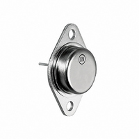
Package / Case
TO-204, TO-3
Transistor Polarity
NPN
Mounting Style
Through Hole
Collector- Emitter Voltage Vceo Max
90 V
Emitter- Base Voltage Vebo
4 V
Maximum Dc Collector Current
30 A
Power Dissipation
200 W
Maximum Operating Temperature
+ 200 C
Continuous Collector Current
30 A
Dc Collector/base Gain Hfe Min
25
Maximum Operating Frequency
2 MHz
Minimum Operating Temperature
- 65 C
Current, Collector
30 A
Current, Gain
100
Frequency
2 MHz
Package Type
TO-204AA (TO-3)
Polarity
PNP
Primary Type
Si
Resistance, Thermal, Junction To Case
0.875 °C/W
Voltage, Breakdown, Collector To Emitter
100 V
Voltage, Collector To Base
100 V
Voltage, Collector To Emitter
100 V
Voltage, Collector To Emitter, Saturation
0.8 V
Voltage, Emitter To Base
90 V
Number Of Elements
1
Collector-emitter Voltage
90V
Collector-base Voltage
100V
Emitter-base Voltage
4V
Collector Current (dc) (max)
30A
Dc Current Gain (min)
25
Frequency (max)
2MHz
Operating Temp Range
-65C to 200C
Operating Temperature Classification
Military
Mounting
Through Hole
Pin Count
2 +Tab
Lead Free Status / RoHS Status
Lead free / RoHS Compliant
Current - Collector Cutoff (max)
-
Lead Free Status / Rohs Status
Lead free / RoHS Compliant
Other names
MJ4502GOS


H
V
E
2
1
−Q−
A
U
N
L
0.13 (0.005)
D
2 PL
0.13 (0.005)
C
G
M
−Y−
K
T
M
−T−
B
Y
T
M
Q
SEATING
PLANE
PACKAGE DIMENSIONS
M
Y
TO−204 (TO−3)
M
CASE 1−07
ISSUE Z
MJ4502
4
NOTES:
1. DIMENSIONING AND TOLERANCING PER ANSI
2. CONTROLLING DIMENSION: INCH.
3. ALL RULES AND NOTES ASSOCIATED WITH
Y14.5M, 1982.
REFERENCED TO−204AA OUTLINE SHALL APPLY.
STYLE 1:
DIM
A
B
C
D
G
H
K
N
Q
U
E
L
V
CASE: COLLECTOR
PIN 1. BASE
2. EMITTER
0.250
0.038
0.055
0.440
0.151
0.131
MIN
−−−
−−−
1.550 REF
0.430 BSC
0.215 BSC
0.665 BSC
1.187 BSC
INCHES
1.050
0.335
0.043
0.070
0.480
0.830
0.165
0.188
MAX
11.18
MILLIMETERS
MIN
6.35
0.97
1.40
3.84
3.33
−−−
−−−
39.37 REF
10.92 BSC
16.89 BSC
30.15 BSC
5.46 BSC
26.67
12.19
21.08
MAX
8.51
1.09
1.77
4.19
4.77
Related parts for MJ4502G
Image
Part Number
Description
Manufacturer
Datasheet
Request
R

Part Number:
Description:
ON Semiconductor [VOLTAGE REGULATOR]
Manufacturer:
ON Semiconductor
Datasheet:
Part Number:
Description:
357-036-542-201 CARDEDGE 36POS DL .156 BLK LOPRO
Manufacturer:
ON Semiconductor
Datasheet:
Part Number:
Description:
357-036-542-201 CARDEDGE 36POS DL .156 BLK LOPRO
Manufacturer:
ON Semiconductor
Datasheet:
Part Number:
Description:
357-036-542-201 CARDEDGE 36POS DL .156 BLK LOPRO
Manufacturer:
ON Semiconductor
Datasheet:
Part Number:
Description:
357-036-542-201 CARDEDGE 36POS DL .156 BLK LOPRO
Manufacturer:
ON Semiconductor
Datasheet:
Part Number:
Description:
357-036-542-201 CARDEDGE 36POS DL .156 BLK LOPRO
Manufacturer:
ON Semiconductor
Datasheet:
Part Number:
Description:
357-036-542-201 CARDEDGE 36POS DL .156 BLK LOPRO
Manufacturer:
ON Semiconductor
Datasheet:
Part Number:
Description:
357-036-542-201 CARDEDGE 36POS DL .156 BLK LOPRO
Manufacturer:
ON Semiconductor
Datasheet:
Part Number:
Description:
357-036-542-201 CARDEDGE 36POS DL .156 BLK LOPRO
Manufacturer:
ON Semiconductor
Datasheet:
Part Number:
Description:
357-036-542-201 CARDEDGE 36POS DL .156 BLK LOPRO
Manufacturer:
ON Semiconductor
Datasheet:
Part Number:
Description:
357-036-542-201 CARDEDGE 36POS DL .156 BLK LOPRO
Manufacturer:
ON Semiconductor
Datasheet:
Part Number:
Description:
Manufacturer:
ON Semiconductor
Datasheet:
Part Number:
Description:
Manufacturer:
ON Semiconductor
Datasheet:
Part Number:
Description:
Manufacturer:
ON Semiconductor
Datasheet: