BD533 STMicroelectronics, BD533 Datasheet
BD533
Specifications of BD533
BD533
Available stocks


Related parts for BD533


BD533 Summary of contents
Page 1
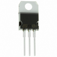
... Features BD533, BD535, and BD537 are NPN transistors Description The devices are manufactured in Planar technology with “Base Island” layout. The resulting transistor shows exceptional high gain performance coupled with very low saturation voltage. The PNP types are BD534 and BD536. ...
Page 2
... Collector current C I Base current B P Total dissipation at T TOT T Storage temperature stg T Max. operating junction temperature J Note: For PNP types voltage and current values are negative 2/11 BD533 BD534 BD535 BD536 BD537 Parameter NPN PNP = 25°C case Value Unit BD533 ...
Page 3
... BD533 BD534 BD535 BD536 BD537 Table 3. Electrical characteristics (T = 25°C; unless otherwise specified) case Table 4. Electrical characteristics Symbol Collector cut-off current I CBO ( Collector cut-off current I CES (V BE Emitter cut-off current I EBO ( Collector-emitter (1) sustaining voltage V CEO(sus Collector-emitter (1) V CE(sat) saturation voltage (1) Base-emitter voltage ...
Page 4
... Absolute maximum ratings 1.1 Electrical characteristic (curves) Figure 2. Safe operating area Figure 4. DC current gain (NPN) Figure 6. DC current gain (NPN) 4/11 BD533 BD534 BD535 BD536 BD537 Figure 3. Derating curve Figure 5. DC current gain (PNP) Figure 7. DC current gain (PNP) ...
Page 5
... BD533 BD534 BD535 BD536 BD537 Figure 8. Collector-emitter saturation voltage (NPN) Figure 10. Base-emitter saturation voltage (NPN) Figure 12. Base-emitter on voltage (NPN) Absolute maximum ratings Figure 9. Collector-emitter saturation voltage (PNP) Figure 11. Base-emitter saturation voltage (PNP) Figure 13. Base-emitter on voltage (PNP) 5/11 ...
Page 6
... Figure 14. Resistive load switching time (NPN) Figure 16. Resistive load switching time (NPN) Figure 18. Collector-base and collector- emitter capacitance (NPN) 6/11 BD533 BD534 BD535 BD536 BD537 Figure 15. Resistive load switching time (PNP) Figure 17. Resistive load switching time (PNP) Figure 19. Collector-base and collector- emitter capacitance (PNP) ...
Page 7
... BD533 BD534 BD535 BD536 BD537 1.2 Test circuits Figure 20. Resistive load switching test circuit 1) Fast electronic switch 2) Non-inductive resistor Absolute maximum ratings 7/11 ...
Page 8
... The category of second level interconnect is marked on the package and on the inner box label, in compliance with JEDEC Standard JESD97. The maximum ratings related to soldering conditions are also marked on the inner box label. ECOPACK trademark. ECOPACK specifications are available at: www.st.com 8/11 BD533 BD534 BD535 BD536 BD537 ...
Page 9
... BD533 BD534 BD535 BD536 BD537 DIM L20 L30 øP Q TO-220 Mechanical data mm. MIN. TYP 4.40 0.61 1.14 0.49 15.25 1.27 10 2.40 4.95 1.23 6.20 2.40 13 3.50 16.40 28.90 3.75 2.65 Package mechanical data MAX. 4.60 0.88 1.70 0.70 15.75 10.40 2.70 5 ...
Page 10
... Revision history 3 Revision history Table 5. Revision history Date 01-Jun-1997 11-Feb-2003 27-Mar-2007 23-Jul-2007 10/11 Revision 1 Initial Release 2 Minor text changes Figure 10, 11, 12, 13, 14, 15, 16, 17, 18, 19 and 3 figure 20 added 4 Figure 2 and figure 3 added BD533 BD534 BD535 BD536 BD537 Changes ...
Page 11
... BD533 BD534 BD535 BD536 BD537 Information in this document is provided solely in connection with ST products. STMicroelectronics NV and its subsidiaries (“ST”) reserve the right to make changes, corrections, modifications or improvements, to this document, and the products and services described herein at any time, without notice. All ST products are sold pursuant to ST’s terms and conditions of sale. ...