BCP68T1G ON Semiconductor, BCP68T1G Datasheet
BCP68T1G
Specifications of BCP68T1G
Available stocks


Related parts for BCP68T1G


BCP68T1G Summary of contents
Page 1
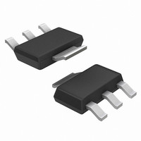
... R 83.3 qJA °C T 260 L 10 Sec BCP68T1 BCP68T1G BCP68T3 BCP68T3G †For information on tape and reel specifications, Preferred devices are recommended choices for future use and best overall value. 1 MEDIUM POWER NPN SILICON HIGH CURRENT TRANSISTOR SURFACE MOUNT COLLECTOR 2,4 BASE ...
Page 2
ELECTRICAL CHARACTERISTICS Characteristics OFF CHARACTERISTICS Collector−Emitter Breakdown Voltage (I C Collector−Emitter Breakdown Voltage ( mAdc, I Emitter−Base Breakdown Voltage (I E Collector−Base Cutoff Current ( Vdc Emitter−Base Cutoff Current (V = 5.0 Vdc, ...
Page 3
... A 0.08 (0003) A1 2.0 0.079 *For additional information on our Pb−Free strategy and soldering details, please download the ON Semiconductor Soldering and Mounting Techniques Reference Manual, SOLDERRM/D. BCP68T1 PACKAGE DIMENSIONS SOT−223 (TO−261) CASE 318E−04 ISSUE L NOTES: 1. DIMENSIONING AND TOLERANCING PER ANSI Y14.5M, 1982. ...