MJE5742G ON Semiconductor, MJE5742G Datasheet

TRANS DARL NPN 8A 400V TO220AB

MJE5742G

Manufacturer Part Number
MJE5742G
Description
TRANS DARL NPN 8A 400V TO220AB
Manufacturer
ON Semiconductor
Type
High Voltage, Powerr
Datasheets

Specifications of MJE5742G

Transistor Type
NPN - Darlington
Current - Collector (ic) (max)
8A
Voltage - Collector Emitter Breakdown (max)
400V
Vce Saturation (max) @ Ib, Ic
3V @ 400mA, 8A
Dc Current Gain (hfe) (min) @ Ic, Vce
200 @ 2A, 5V
Power - Max
2W
Mounting Type
Through Hole
Package / Case
TO-220-3 (Straight Leads)
Configuration
Single
Transistor Polarity
NPN
Mounting Style
Through Hole
Collector- Emitter Voltage Vceo Max
400 V
Emitter- Base Voltage Vebo
8 V
Maximum Dc Collector Current
8 A
Power Dissipation
2 W
Maximum Operating Temperature
+ 150 C
Continuous Collector Current
8 A
Dc Collector/base Gain Hfe Min
200, 50
Minimum Operating Temperature
- 65 C
Current, Gain
400
Current, Input
2.5 A
Current, Output
8 A
Package Type
TO-220AB
Polarity
NPN
Primary Type
Si
Resistance, Thermal, Junction To Ambient
62.5
Voltage, Collector To Emitter, Saturation
3 V
Voltage, Input
8 V
Voltage, Output
400 V
Lead Free Status / RoHS Status
Lead free / RoHS Compliant
Current - Collector Cutoff (max)
-
Frequency - Transition
-
Lead Free Status / Rohs Status
Lead free / RoHS Compliant
Other names
MJE5742GOS

Available stocks

Company
Part Number
Manufacturer
Quantity
Price
Part Number:
MJE5742G
Manufacturer:
ON Semiconductor
Quantity:
1 862
Part Number:
MJE5742G
Manufacturer:
FSC
Quantity:
2 000
MJE5740, MJE5742
NPN Silicon Power
Darlington Transistors
high−voltage power switching in inductive circuits.
Features
Applications
Maximum ratings are those values beyond which device damage can occur.
Maximum ratings applied to the device are individual stress limit values (not
normal operating conditions) and are not valid simultaneously. If these limits are
exceeded, device functional operation is not implied, damage may occur and
reliability may be affected.
1. Pulse Test: Pulse Width = 5 ms, Duty Cycle ≤ 10%.
*For additional information on our Pb−Free strategy and soldering details, please
MAXIMUM RATINGS
THERMAL CHARACTERISTICS
download the ON Semiconductor Soldering and Mounting Techniques
Reference Manual, SOLDERRM/D.
Collector−Emitter Voltage
Emitter−Base Voltage
Collector Current
Base Current
Total Device Dissipation @ T
Derate above 25°C
Total Device Dissipation @ T
Derate above 25°C
Operating and Storage Junction
Temperature Range
Thermal Resistance, Junction−to−Case
Thermal Resistance, Junction−to−Ambient
Maximum Lead Temperature for Soldering
Purposes 1/8″ from Case for 5 Seconds
The MJE5740 and MJE5742 Darlington transistors are designed for
Pb−Free Packages are Available*
Small Engine Ignition
Switching Regulators
Inverters
Solenoid and Relay Drivers
Motor Controls
Characteristics
Rating
− Continuous
− Peak (Note 1)
− Continuous
− Peak (Note 1)
MJE5742 is a Preferred Device
C
C
= 25_C
= 25_C
MJE5740
MJE5742
MJE5740
MJE5742
V
Symbol
Symbol
T
CEO(sus)
V
R
R
J
V
I
I
P
P
CEV
, T
T
CM
BM
I
I
qJC
qJA
EB
C
B
D
D
L
stg
−65 to +150
Value
Max
1.25
62.5
300
400
600
800
640
275
2.5
16
16
80
8
8
5
2
1
W/_C
W/_C
_C/W
_C/W
Unit
Unit
Vdc
Vdc
Vdc
Adc
Adc
_C
_C
W
W
See detailed ordering and shipping information in the package
dimensions section on page 2 of this data sheet.
Preferred devices are recommended choices for future use
and best overall value.
1
2
3
POWER DARLINGTON
MJE574x
G
A
Y
WW
ORDERING INFORMATION
300−400 VOLTS
CASE 221A−09
TRANSISTORS
BASE
TO−220AB
8 AMPERES
STYLE 1
1
80 WATTS
≈ 100
COLLECTOR 2,4
= Device Code
= Pb−Free Package
= Assembly Location
= Year
= Work Week
x = 0 or 2
EMITTER 3
≈ 50
MARKING
DIAGRAM
MJE574xG
AY WW

Related parts for MJE5742G

MJE5742G Summary of contents

Page 1

... Pulse Test: Pulse Width = 5 ms, Duty Cycle ≤ 10%. *For additional information on our Pb−Free strategy and soldering details, please download the ON Semiconductor Soldering and Mounting Techniques Reference Manual, SOLDERRM/D. Symbol Value ...

Page 2

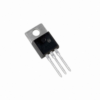
... The internal Collector−to−Emitter diode can eliminate the need for an external diode to clamp inductive loads. Tests have shown that the Forward Recovery Voltage ( this diode is comparable to that of typical fast recovery rectifiers. f ORDERING INFORMATION Device MJE5740 MJE5740G MJE5742 MJE5742G (T = 25_C unless otherwise noted) C Î Î Î Î Î Î Î Î Î Î Î Î MJE5740 MJE5742 Î ...

Page 3

PACKAGE DIMENSIONS TO−220AB CASE 221A−09 ISSUE AA NOTES: SEATING −T− 1. DIMENSIONING AND TOLERANCING PER ANSI PLANE Y14.5M, 1982 CONTROLLING ...

Related keywords