2N3055AG ON Semiconductor, 2N3055AG Datasheet

TRANSISTOR NPN 60V 15A BIPO TO-3

2N3055AG

Manufacturer Part Number
2N3055AG
Description
TRANSISTOR NPN 60V 15A BIPO TO-3
Manufacturer
ON Semiconductor
Type
High Powerr
Datasheets

Specifications of 2N3055AG

Transistor Type
NPN
Current - Collector (ic) (max)
15A
Voltage - Collector Emitter Breakdown (max)
60V
Vce Saturation (max) @ Ib, Ic
5V @ 7A, 15A
Current - Collector Cutoff (max)
700µA
Dc Current Gain (hfe) (min) @ Ic, Vce
10 @ 4A, 2V
Power - Max
115W
Frequency - Transition
6MHz
Mounting Type
Chassis Mount
Package / Case
TO-204, TO-3
Transistor Polarity
NPN
Mounting Style
Through Hole
Collector- Emitter Voltage Vceo Max
60 V
Emitter- Base Voltage Vebo
7 V
Maximum Dc Collector Current
15 A
Power Dissipation
115 W
Maximum Operating Temperature
+ 200 C
Continuous Collector Current
15 A
Dc Collector/base Gain Hfe Min
10
Maximum Operating Frequency
6 MHz
Minimum Operating Temperature
- 65 C
Current, Collector
15 A
Current, Gain
5
Frequency
0.8 MHz
Package Type
TO-204AA (TO-3)
Polarity
NPN
Primary Type
Si
Resistance, Thermal, Junction To Case
1.52 °C/W
Voltage, Breakdown, Collector To Emitter
60 V
Voltage, Collector To Base
100 V
Voltage, Collector To Emitter
60 V
Voltage, Collector To Emitter, Saturation
5 V
Voltage, Emitter To Base
7 V
Lead Free Status / RoHS Status
Lead free / RoHS Compliant
Other names
2N3055AG
2N3055AGOS

Available stocks

Company
Part Number
Manufacturer
Quantity
Price
Part Number:
2N3055AG
Manufacturer:
ON/安森美
Quantity:
20 000
2N3055A (NPN),
MJ15015 (NPN),
MJ15016 (PNP)
Complementary Silicon
High−Power Transistors
high power audio, stepping motor and other linear applications. These
devices can also be used in power switching circuits such as relay or
solenoid drivers, dc−to−dc converters, inverters, or for inductive loads
requiring higher safe operating area than the 2N3055.
Features
Stresses exceeding Maximum Ratings may damage the device. Maximum
Ratings are stress ratings only. Functional operation above the Recommended
Operating Conditions is not implied. Extended exposure to stresses above the
Recommended Operating Conditions may affect device reliability.
1. Indicates JEDEC Registered Data. (2N3055A)
*For additional information on our Pb−Free strategy and soldering details, please
MAXIMUM RATINGS
THERMAL CHARACTERISTICS
© Semiconductor Components Industries, LLC, 2006
April, 2006 − Rev. 6
Collector−Emitter Voltage
Collector−Base Voltage
Collector−Emitter Voltage Base
Reversed Biased
Emitter−Base Voltage
Collector Current − Continuous
Base Current
Total Device Dissipation @ T
Derate above 25_C
Total Device Dissipation @ T
Derate above 25_C
Operating and Storage Junction
Temperature Range
Thermal Resistance, Junction−to−Case
download the ON Semiconductor Soldering and Mounting Techniques
Reference Manual, SOLDERRM/D.
These PowerBaset complementary transistors are designed for
Current−Gain − Bandwidth−Product @ I
Safe Operating Area − Rated to 60 V and 120 V, Respectively
Pb−Free Packages are Available*
f
T
Characteristics
= 0.8 MHz (Min) − NPN
= 2.2 MHz (Min) − PNP
MJ15015 and MJ15016 are Preferred Devices
Rating
MJ15015, MJ15016
MJ15015, MJ15016
MJ15015, MJ15016
MJ15015, MJ15016
(Note 1)
C
C
2N3055A
2N3055A
2N3055A
= 25_C
2N3055A
= 25_C
Symbol
Symbol
T
V
V
V
V
R
J
P
, T
CEO
CBO
EBO
CEV
I
I
qJC
C
C
B
D
stg
= 1.0 Adc
−65 to +200
Max
1.52
Value
0.65
1.03
120
100
200
100
200
180
115
7.0
7.0
60
15
Max
0.98
1
W/_C
_C/W
Unit
Unit
Vdc
Vdc
Vdc
Vdc
Adc
Adc
_C
W
60, 120 VOLTS − 115, 180 WATTS
See detailed ordering and shipping information in the package
dimensions section on page 5 of this data sheet.
Preferred devices are recommended choices for future use
and best overall value.
COMPLEMENTARY SILICON
POWER TRANSISTORS
2N3055AG
ORDERING INFORMATION
2N3055A = Device Code
MJ1501x = Device Code
G
A
Y
WW
MEX
AYWW
MEX
MARKING DIAGRAMS
http://onsemi.com
15 AMPERE
TO−204AA (TO−3)
CASE 1−07
= Pb−Free Package
= Assembly Location
= Year
= Work Week
= Country of Origin
STYLE 1
x = 5 or 6
Publication Order Number:
MJ1501xG
AYWW
MEX
2N3055A/D

Related parts for 2N3055AG

2N3055AG Summary of contents

Page 1

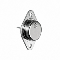
... Preferred devices are recommended choices for future use and best overall value. 1 http://onsemi.com 15 AMPERE COMPLEMENTARY SILICON POWER TRANSISTORS TO−204AA (TO−3) CASE 1−07 STYLE 1 MARKING DIAGRAMS 2N3055AG MJ1501xG AYWW AYWW MEX MEX 2N3055A = Device Code MJ1501x = Device Code Pb−Free Package A ...

Page 2

MJ15015 (NPN), MJ15016 (PNP) Î Î Î Î Î Î Î Î Î Î Î Î Î Î Î Î Î Î Î Î Î Î Î Î Î Î Î Î Î Î Î Î Î ELECTRICAL ...

Page 3

MJ15015 (NPN), MJ15016 (PNP) 200 150 100 200 T = 150°C J 100 70 50 −55 ° 25° 4 0.2 0.3 0.5 0.7 1 ...

Page 4

MJ15015 (NPN), MJ15016 (PNP + −11 V ≤ −5 V DUTY CYCLE = 1.0% Figure 6. Switching Times Test Circuit (Circuit shown is for NPN) ...

Page 5

... Safe Operating area curves indicate I limits of the transistor that must be observed for reliable operation; i.e., the transistor must not be subjected to greater dissipation than the curves indicate. ORDERING INFORMATION Device 2N3055A 2N3055AG MJ15015 MJ15015G MJ15016 MJ15016G COLLECTOR CUT−OFF REGION PNP ...

Page 6

... American Technical Support: 800−282−9855 Toll Free USA/Canada Japan: ON Semiconductor, Japan Customer Focus Center 2−9−1 Kamimeguro, Meguro−ku, Tokyo, Japan 153−0051 Phone: 81−3−5773−3850 http://onsemi.com 6 NOTES: 1. DIMENSIONING AND TOLERANCING PER ANSI Y14.5M, 1982. 2. CONTROLLING DIMENSION: INCH. ...

Related keywords