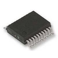
ATA5743P6-TKQY 19 Atmel, ATA5743P6-TKQY 19 Datasheet - Page 20

ATA5743P6-TKQY 19
Manufacturer Part Number
ATA5743P6-TKQY 19
Description
RF Receiver UHF ASK / FSK Receiver
Manufacturer
Atmel
Type
Receiverr
Datasheet
1.ATA5743P3-TGQY.pdf
(43 pages)
Specifications of ATA5743P6-TKQY 19
Package / Case
SSO-20
Operating Frequency
449 MHz
Operating Supply Voltage
4.5 V to 5.5 V
Maximum Operating Temperature
+ 105 C
Minimum Operating Temperature
- 40 C
Mounting Style
SMD/SMT
Noise Figure
7 dB
Lead Free Status / RoHS Status
Lead free / RoHS Compliant
Figure 6-14. Timing Diagram of the Data Clock
Figure 6-15. Data Clock Disappears Because of a Timing Error
20
ATA5743
Dem_out
Data_out (DATA)
DATA_CLK
Dem_out
Data_out (DATA)
DATA_CLK
The limits for 2T are calculated as follows:
Lower limit of 2T: Lim_min_2T = (Lim_min + Lim_max) - (Lim_max - Lim_min)/2
Upper limit of 2T: Lim_max_2T = (Lim_min + Lim_max) + (Lim_max - Lim_min)/2
Note:
The data clock is available after the data clock control logic has detected the distance 2T (Start
bit), and then issues pulses with a delay of t
If the data clock control logic detects a timing or logical error (Manchester code violation), as
illustrated in
receiver remains in receiving mode and starts with the bit check. If the bit check was successful
and the start bit has been detected, the data clock control logic starts again with the generation
of the data clock (see
It is recommended to use the function of the data clock only in conjunction with the bit check 3, 6
or 9. If the bit check is set to 0 or the receiver is set to receiving mode via the pin POLLING/_ON,
the data clock is available if the data clock control logic has detected the distance 2T (Start bit).
Note that for Bi-phase-coded signals, the data clock is issued at the end of the bit.
If the result for “Lim_min_2T” or “Lim_max_2T” is not an integer value, it will be rounded up.
1
1
Receiving mode,
data clock control
logic active
Bit check ok
Bit-check mode
Timing error
Figure 6-15
1
1
Figure 6-17 on page
1
1
T
(
T
ee
and
ee
Preburst
< T
1
1
Lim_min
Figure 6-16 on page
T
OR T
1
1
2T
Lim_max
Start bit
Data
0
0
21).
Delay
< T
Receiving mode,
bit check active
ee
data clock control logic active
1
1
after the edges on pin DATA (see
< T
Receiving mode,
21, it stops the output of the data clock. The
Lim_min_2T
1
1
t
Delay
Data
OR T
0
0
ee
> T
1
1
Lim_max_2T
t
P_Data_Clk
0
0
)
4839B–RKE–08/05
Figure
6-14).


