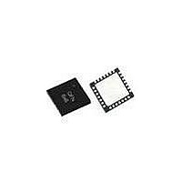
CV110-3AF TriQuint, CV110-3AF Datasheet - Page 2

CV110-3AF
Manufacturer Part Number
CV110-3AF
Description
Up-Down Converters 800-960MHz RF 200-350MHz IF
Manufacturer
TriQuint
Type
Down Converterr
Datasheet
1.CV110-3APCB240.pdf
(4 pages)
Specifications of CV110-3AF
If Frequency
65 MHz to 120 MHz
Maximum Input Frequency
960 MHz
Mounting Style
SMD/SMT
Noise Figure
5 dB
Operating Current
360 mA
P1db
20.3 dBm
Rf Frequency
800 MHz to 960 MHz
Maximum Operating Frequency
350 MHz
Operating Supply Voltage
5 V
Maximum Operating Temperature
+ 85 C
Minimum Operating Temperature
- 40 C
Package / Case
QFN-28 EP
Lead Free Status / RoHS Status
Lead free / RoHS Compliant
Other names
1066931
Available stocks
Company
Part Number
Manufacturer
Quantity
Price
Company:
Part Number:
CV110-3AF
Manufacturer:
TriQuint
Quantity:
33
Part Number:
CV110-3AF
Manufacturer:
TRIQUINT
Quantity:
20 000
CV110-3A: The application circuit can be broken up into four main
functions as denoted in the colored dotted areas above: RF/IF
diplexing (purple), amplifier matching (green), filtering (red), and dc
biasing (blue). There are various placeholders for chip components in
the circuit schematic so that a common PCB can be used for all WJ
single-branch converters. Additional placeholders for other optional
functions such as filtering are also included.
RF / IF Amplifier Matching:
matching element for optimal gain and input return loss performance.
The IF amplifier requires matching elements to optimize the
performance of the amplifier to the desired IF center frequency.
Since IF bandwidths are typically on the order of 5 to 10%, a simple
two element matching network, in the form of either a high-pass or
low-pass filter structure, is sufficient to match the MMIC IF
amplifier over these narrow bandwidths. Proper component values for
other IF center frequencies can be found in the IF Amplifier Matching
Table or by e-mailing to
RF Bandpass Filtering:
reject the image frequencies and achieve the best noise figure
TriQuint Semiconductor, Inc • Phone 1-800-WJ1-4401 • FAX: 408-577-6633 • e-mail: info-sales@tqs.com • Web site: www.TriQuint.com
IF THRU
RF OUT
RF/IF
GND
GND
GND
N/C
1
2
3
4
5
6
7
RF/IF
RF Amp
RF Bandpass Filter /
28
8
Attenuator Pad
CV110-3A
Cellular-band High Linearity Downconverter
IF Feedthru
27
9
Path
(used for cellular versions only)
26
10
Frequency (MHz)
Device Architecture / Application Circuit Information
25
11
RF / IF Diplexer
sjcapplication.engineering@tqs.com
LO
RF Amp Bias
R8 (ohms)
24
12
C17 (pF)
LO Driver Amp
L7 (nH)
L4 (nH)
Bandpass filtering is recommended to
23
13
IF Amp
22
14
The RF amplifier requires a shunt
RF Amp Matching
21
20
19
18
17
16
15
IF OUT
GND
N/C
GND
BIAS
GND
LO IN
470
470
4.7
40
24
MMIC Mixer
RF Amplifier
IF Amplifier
CV110-3A
RF Filter
430
240
IF Amp Matching
4.7
50
15
Stage
IF Amplifier Matching
150
330
3.3
75
22
LO Amp Bias
Gain
(dB)
13.5
19.0
-1.5
-9.0
IF Amp Bias
.
100
150
330
2.2
Typical Downconverter Performance Chain Analysis
10
Cumulative Performance
LO Amp Bias
Output
(dBm)
P1dB
125
120
330
21
---
22
8.2
2.2
8
performance with the downconverter.
implemented with a SAW filter on the application circuit, allows for
the suppression of noise from the image frequency. It is permissible
to not use a filter and use a 2 dB pad with R6, R7, and R16 instead
with slightly degraded noise figure performance.
evaluation boards will have the 2 dB pad in place.
External Diplexer:
RF signal impinges on the switching elements of the mixer; the
interaction with these switches produces a signal at the IF frequency.
The two signals (RF and IF) are directed to the appropriate ports by
the external diplexer. Pin 5 contains the IF signal and allows the
signal to be transferred to pin 25 for the convenience of PCB layouts.
DC biasing:
amplifiers in the converter. R1 sets the operating current for the last
stage of the LO amplifier and is chosen to optimize the mixer LO
drive level. Proper RF chokes and bypass capacitors are chosen for
proper amplifier biasing at the intended frequency of operation. The
“+5 V” dc bias should be supplied directly from a voltage regulator.
130
120
330
Output
6.8
2.2
(dBm)
40.0
23.0
39.1
IP3
---
Printed Circuit Board Material:
.014” FR-4, 4 layers, .062” total thickness
155
100
330
5.6
2.2
DC bias must be provided for the RF, LO and IF
(dB)
NF
9.8
3.5
1.5
2.5
Specifications and information are subject to change without notice
In a downconversion application, the incoming
169
330
5.0
2.2
82
Current
(mA)
150
150
360
---
60
180
330
4.7
2.2
82
Gain
(dB)
13.5
12.0
22.0
22.0
3.0
210
220
3.3
2.2
82
Cumulative Performance
Output
(dBm)
P1dB
21.0
19.5
20.3
20.3
240
220
6.1
3.9
2.2
56
The bandpass filter,
Page 2 of 4 October 2008
Output
(dBm)
40.0
38.5
22.1
37.0
37.0
IP3
Standard WJ
(dB)
NF
4.5
5.0
3.5
3.5
5.0


