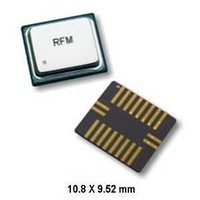
TR3100 RFM, TR3100 Datasheet
TR3100
Specifications of TR3100


Related parts for TR3100


TR3100 Summary of contents
Page 1
... A wide dynamic range log detector, in combination with digital AGC and a compound data slicer, provide robust performance in the presence of on-channel interference or noise. Two stages of SAW filtering provide excellent receiver out-of-band rejection. The TR3100 is optimized for RF data rates from 230.4 to 576 kbps using amplitude-shift keyed (ASK) modulation. The transmitter employs SAW filtering to suppress output harmonics, facilitating compliance with ETSI I-ETS 300 220 and similar regulations ...
Page 2
... Vdc mV 10 P-P 85 ° Inches Min Nom Max .425 .430 .435 .375 .380 .385 .070 .075 .080 .120 .125 .130 .015 .020 .025 .035 .040 .045 .125 .130 .135 .070 .075 0.80 Page TR3100 - 4/4/08 ...
Page 3
... K ±1% 100 K ±1%, for 6 dB below peak 27 K ±1%, typical values 22 K ±5% K ±5% 4.7 µF tantalum 100 pF ±5% NPO 100 pF ±5% NPO vendor 2506033017YO or equivalent ohm antenna 6.8 pF ±5% NPO 220 nH 50 ohm antenna Notes Page TR3100 - 4/4/08 ...
Page 4
... RFA1 is ON (up to 50%). SAW SAW Filter RFA1 Delay Line P1 Pulse Generator RF Data Pulse t PRI t PRC Figure 1 (RFA1 duty factor), where the 10 Detector & Data RFA2 Low-Pass Out Filter P2 Page TR3100 - 4/4/08 ...
Page 5
... CMPIN by separate series coupling capacitors. The AGC reset function is driven by the signal applied to CMPIN. BBOUT DS2 Ref Peak Detector C BBO dB Below PKDET 4 Peak Thld C PKD AGC DS1 Ref Thld Threshold Control THLD1 THLD2 R R TH1 TH2 R REF AND RXDATA 7 Page TR3100 - 4/4/08 ...
Page 6
... Transmitter operation supports two modulation formats, on-off keyed (OOK) modulation, and amplitude-shift keyed (ASK) modulation which is normally used by the TR3100. When OOK modulation is chosen, the transmitter output turns completely off between “1” data pulses. When ASK modulation is chosen, a “1” ...
Page 7
... K. The value of the 404 the high data rate mode normally used by the TR3100 (selected at the PWIDTH pin) the receiver RF amplifiers operate at a nominal 50%-50% duty cycle. In this case, the period pulse to the first RF amplifier to the start of the next ON pulse to the first RF amplifier is controlled by the PRATE resistor over a range of 0.1 to 1.1 µ ...
Page 8
... PKA and t in µs slaved to attack time PKA user selected mode user selected mode user selected mode user selected mode user selected mode in kHz user selected LPF in kilohms user selected LPF in pF user selected BBO Notes PKD Page TR3100 - 4/4/08 ...
Page 9
... MAX MAX Description , the capacitor value C AGH given above provides a hold-in time between t AGC , the capacitor value C is: BBO PKD and 1.5* t PKA For this case: MAX BBO AGC AGH with variations PKA for internal BBO and BBC Page TR3100 - 4/4/08 ...
Page 10
... O A ±5% resistor value is recommended. In the ASK mode (TR3100), this pin accepts analog modulation (shaped or unshaped data pulses). ASK modulation is practical for data pulses 1 µs or longer. The resistor driving this pin must be low in the receive and power-down (sleep) modes. Please refer to the ASH Transceiver Designer’s Guide for additional information on modulation techniques ...
Page 11
... RF amplifier). The ON pulse width t PW2 - 18.6, where µs and kilohms PW1 PW1 PW SM-20L PCB Pad Layout .4600 0.000 Dimensions in inches with a resistor R to ground (the ON pulse PW1 PW is given by: PW .3825 .3575 .3175 .2775 .2375 .1975 .1575 .1175 .1025 .0775 Page TR3100 - 4/4/08 PW1 ...
Page 12
... RF Monolithics, Inc. RF Output Power 100 125 150 175 I in µA TXM TXM TXM 50 75 100 125 150 175 I in µA TXM Note: Specifications subject to change without notice. TXM 3 V 200 225 250 275 200 225 250 275 Page TR3100 - 4/4/08 ...