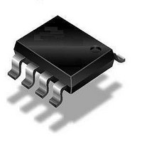
ATA6661-TAQJ Atmel, ATA6661-TAQJ Datasheet - Page 11

ATA6661-TAQJ
Manufacturer Part Number
ATA6661-TAQJ
Description
RF Transceiver LIN Transceiver
Manufacturer
Atmel
Datasheet
1.ATA6661-TAQJ_19.pdf
(16 pages)
Specifications of ATA6661-TAQJ
Mounting Style
SMD/SMT
Package / Case
SOIC
Lead Free Status / RoHS Status
Lead free / RoHS Compliant
Available stocks
Company
Part Number
Manufacturer
Quantity
Price
Company:
Part Number:
ATA6661-TAQJ
Manufacturer:
ATMEL
Quantity:
48 145
Part Number:
ATA6661-TAQJ
Manufacturer:
ATMEL/爱特梅尔
Quantity:
20 000
Part Number:
ATA6661-TAQJ19
Manufacturer:
ATMEL/爱特梅尔
Quantity:
20 000
6. Electrical Characteristics (Continued)
5V < V
4729M–AUTO–02/09
*) Type means: A = 100% tested, B = 100% correlation tested, C = Characterized on samples, D = Design parameter
10.1
10.2
10.3
10.4
11.1
11.2
No.
8.6
8.7
9.1
9.2
9.3
9.4
9.5
9.6
10
11
9
S
< 18V, T
Parameters
Wake detection LIN
Low level input voltage
LIN pull-up current
Internal Timers
Dominant time for wake-up via
LIN bus
Time of low pulse for wake-up
via pin WAKE
Time delay for mode change
from pre-normal mode to normal
mode via pin EN
Time delay for mode change
from normal mode into sleep
mode via pin EN
TXD dominant time out timer
Power-up delay between
V
high
LIN Bus Driver (see
Bus load conditions: Load1 small 1 nF 1 k , Load2 big 10 nF 500 , R
The following two rows specifies the timing parameters for proper operation at 20.0 Kbit/s.
Slope time falling and rising
edge at LIN
Symmetry of rising and falling
edge
Receiver Electrical AC Parameters of the LIN Physical Layer
LIN receiver, RXD load conditions (C
Propagation delay of receiver
(see
Symmetry of receiver
propagation delay rising edge
minus falling edge
Duty cycle 1
Duty cycle 1
S
= 5V until INH switches to
Figure 6-1 on page
amb
= –40°C to +125°C
Figure 6-1 on page
12)
Test Conditions
I
V
V
V
V
V
V
V
TH
TH
V
t
D1 = t
TH
TH
V
t
D2 = t
Load1/Load2
V
VS = 7.3V
t
t
t
LIN
Bit
Bit
sym
rec_pd
rx_sym
S
LIN
WAKE
EN
EN
TXD
VS
S
S
S
Rec(max)
Dom(max)
Rec(min)
Dom(min)
RXD
< 27V
= 7.0V to 18V
= 50 µs
= 7.0V to 18V
= 50 µs
= 7.3V to 18V
= Typically –3 µA
= t
= 5V
= 0V
= 5V
= 0V
= 0V
bus_rec(min)
bus_rec(max)
= max(t
): 20 pF, R
= t
= 0V
Slope_fall
12)
rx_pdr
= 0.422
= 0.744
= 0.284
= 0.581
rx_pdr
– t
– t
/(2
/(2
pull-up
rx_pdf
Slope_rise
, t
rx_pdf
V
t
V
V
t
Bit
V
Bit
= 5 k
S
S
S
S
)
)
)
Pin
6
6
6
3
2
2
4
6
6
6
RXD
Symbol
t
t
Slope_rise
Slope_fall
t
= 5 k , C
t
V
t
t
rx_sym
t
t
WAKE
t
t
rx_pd
I
norm
sleep
BUS
t
D1
D2
dom
sym
LINL
LIN
VS
RXD
0.396
–27V
Min.
–30
3.5
30
60
–4
–2
= 20 pF;
2
2
6
Typ.
–10
130
90
10
10
9
0.581
Max.
V
22.5
150
200
200
3V
15
12
20
+4
+2
S
6
–
ATA6661
Unit
ms
µA
µs
µs
µs
µs
µs
µs
µs
µs
µs
V
Type*
A
A
A
A
A
A
A
A
A
A
A
A
A
A
11


