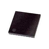
ATA5811-PLQW Atmel, ATA5811-PLQW Datasheet - Page 28

ATA5811-PLQW
Manufacturer Part Number
ATA5811-PLQW
Description
RF Transceiver RF DATA CONTROL Transceiver
Manufacturer
Atmel
Datasheet
1.ATA5811-PLHC.pdf
(92 pages)
Specifications of ATA5811-PLQW
Operating Supply Voltage
2.5 V, 3.3 V, 5 V
Mounting Style
SMD/SMT
Package / Case
QFN-48 EP
Minimum Operating Temperature
- 40 C
Operating Temperature (min)
-40C
Operating Temperature (max)
105C
Operating Temperature Classification
Industrial
Product Depth (mm)
7mm
Product Height (mm)
0.9mm
Product Length (mm)
7mm
Lead Free Status / RoHS Status
Lead free / RoHS Compliant
Available stocks
Company
Part Number
Manufacturer
Quantity
Price
Company:
Part Number:
ATA5811-PLQW
Manufacturer:
ATMEL
Quantity:
971
Part Number:
ATA5811-PLQW
Manufacturer:
ATMEL/爱特梅尔
Quantity:
20 000
28
ATA5811/ATA5812
The supply voltage range of the ATA5811/ATA5812 is 2.4V to 3.6V or 4.4V to 6.6V.
Pin VS1 is the supply voltage input for the range 2.4V to 3.6V and is used in battery applications
using a single lithium 3V cell. Pin VS2 is the voltage input for the range 4.4V to 6.6V (2 Battery
Application and Car Applications) in this case the voltage regulator V_REG1 regulates VS1 to
typically 3.25 V. If the voltage regulator is active a blocking capacitor of 2.2 µF has to be con-
nected to VS1.
Pin VAUX is an input for an additional auxiliary voltage supply and can be connected e.g., to an
inductive supply (see
fier or as in the application of
Pin VSINT is the voltage input for the Microcontoller_Interface and must be connected to the
power supply of the microcontroller. The voltage range of V
on page 32
AVCC is the internal operation voltage of the RF transceiver and is feed via the switch
SW_AVCC by VS1. AVCC must be blocked with a 68 nF capacitor (see
Figure 3-1 on page 7
DVCC is the internal operation voltage of the digital control logic and is feed via the switch
SW_DVCC by VS1 or VSOUT. DVCC must be blocked on pin DVCC with 68 nF (see
on page
Pin VSOUT is a power supply output voltage for external devices (e.g., microcontroller) and is
fed via the switch SW_VSOUT by VS1 or via V_REG2 by the a auxiliary voltage supply VAUX.
The voltage regulator V_REG2 regulates VSOUT to typically 3.25V. If the voltage regulator is
active a blocking capacitor of 2.2 µF has to be connected to VSOUT. VSOUT can be switched
off by the VSOUT_EN bit in control register 3 and is then reactivated by conditions found in
ure 7-2 on page
Pin N_RESET is set to low if the voltage V
can be used as a reset signal for a connected microcontroller (see
Figure 7-4 on page
Pin PWR_ON is an input to switch on the transceiver (active high).
Pin T1 to T5 are inputs for push buttons and can also be used to switch on the transceiver
(active low).
For current consumption reasons it is recommended to set T1 to T5 to GND or PWR_ON to VCC
only temporarily. Otherwise an additional current flows.
There are two voltage monitors generating the following signals (see
• DVCC_OK if DVCC > 1.5V typically
• VSOUT_OK if VSOUT > V
• Low_Batt if VSOUT < V
6,
Figure 3-1 on page 7
and
Figure 7-6 on page
29.
32).
and
Figure 7-6 on page
Figure 4-1 on page
Thres2
Figure 3-1 on page 7
Thres1
(2.38V typically)
and
(2.3V typically)
33).
Figure 4-1 on page
33). This input can only be used together with a recti-
VSOUT
8).
at pin VSOUT drops below 2.3V (typically) and
and must otherwise be left open.
8).
VSINT
is 2.4V to 5.25V (see
Figure 7-3 on page 31
Figure 7-1 on page
Figure 2-1 on page
4689F–RKE–08/06
Figure 7-5
Figure 2-1
27):
Fig-
and
6,


