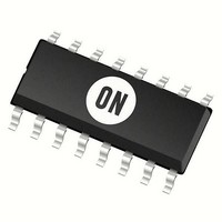
MC74HC4046AD ON Semiconductor, MC74HC4046AD Datasheet - Page 3

MC74HC4046AD
Manufacturer Part Number
MC74HC4046AD
Description
Phase Locked Loops (PLL) LOG CMOS PLL
Manufacturer
ON Semiconductor
Type
PLLr
Datasheet
1.MC74HC4046AD.pdf
(18 pages)
Specifications of MC74HC4046AD
Number Of Circuits
1
Supply Voltage (max)
6 V
Supply Voltage (min)
2 V
Maximum Operating Temperature
+ 125 C
Minimum Operating Temperature
- 55 C
Mounting Style
SMD/SMT
Operating Supply Voltage
2.5 V, 3.3 V, 5 V
Package / Case
SOIC-16
Lead Free Status / RoHS Status
Lead free / RoHS Compliant
Available stocks
Company
Part Number
Manufacturer
Quantity
Price
Company:
Part Number:
MC74HC4046ADR2
Manufacturer:
ON
Quantity:
2 263
Company:
Part Number:
MC74HC4046ADR2G
Manufacturer:
ON Semiconductor
Quantity:
2 000
Company:
Part Number:
MC74HC4046ADTR2G
Manufacturer:
ON Semiconductor
Quantity:
2 000
NOTE: Information on typical parametric values can be found in Chapter 2 of the ON Semiconductor High−Speed CMOS Data Book
[Phase Comparator Section]
DC ELECTRICAL CHARACTERISTICS
Symbol
[Phase Comparator Section]
AC ELECTRICAL CHARACTERISTICS
Symbol
t
t
t
t
t
t
V
t
t
t
t
t
t
V
PZH
V
PLH
PLH
PLH
PLZ
TLH
V
I
I
PHZ
PHL
PHL
PHL
PZL
THL
I
CC
OZ
OH
OL
in
IH
IL
,
,
,
,
,
,
(DL129/D).
Minimum High−Level Input
Voltage DC Coupled
SIG
Maximum Low−Level Input
Voltage DC Coupled
SIG
Minimum High−Level
Output Voltage
PCP
Maximum Low−Level
Output Voltage Qa−Qh
PCP
Maximum Input Leakage Current
SIG
Maximum Three−State
Leakage Current
PC2
Maximum Quiescent Supply Current
(per Package) (VCO disabled)
Pins 3, 5 and 14 at V
Pin 9 at GND; Input Leakage at
Pins 3 and 14 to be excluded
Maximum Propagation Delay, SIG
Maximum Propagation Delay, SIG
Maximum Propagation Delay, SIG
Maximum Propagation Delay, SIG
Maximum Propagation Delay, SIG
Maximum Output Transition Time
(Figure 2)
(Figure 2)
(Figure 2)
Disable Time to PC2
Enable Time to PC2
(Figure 2)
IN
IN
OUT
IN
OUT
, COMP
, COMP
OUT
, COMP
, PCn
, PCn
Parameter
IN
IN
OUT
IN
OUT
CC
OUT
OUT
(Figures 3 and 4)
(Figures 3 and 4)
Parameter
(Voltages Referenced to GND)
(C
IN
IN
IN
IN
IN
/COMP
/COMP
/COMP
/COMP
/COMP
L
V
|I
V
|I
V
|I
V
|I
|I
V
|I
V
|I
|I
V
Output in High−Impedance State
V
V
V
|I
= 50 pF, Input t
out
out
out
out
out
out
out
out
out
out
out
in
in
out
in
in
in
out
in
= V
= V
= V
= V
= V
= V
| ≤ 20 mA
| ≤ 20 mA
| ≤ 20 mA
| ≤ 4.0 mA
| ≤ 5.2 mA
| ≤ 20 mA
| ≤ 4.0 mA
| ≤ 5.2 mA
| = 0 mA
= 0.1 V or V
= 0.1 V or V
= 0.1 V or V
= V
IN
IN
IN
IN
IN
Test Conditions
IH
IH
IH
CC
IH
CC
http://onsemi.com
MC74HC4046A
to PC1
to PCP
to PC3
Output
Output
CC
or V
or V
or V
or V
or GND
or GND
or GND
IL
IL
IL
IL
OUT
OUT
OUT
r
CC
CC
CC
= t
3
f
− 0.1 V
− 0.1 V
− 0.1 V
= 6.0 ns)
V
V
2.0
4.5
6.0
2.0
4.5
6.0
2.0
4.5
6.0
4.5
6.0
2.0
4.5
6.0
4.5
6.0
2.0
3.0
4.5
6.0
6.0
6.0
2.0
4.5
6.0
2.0
4.5
6.0
2.0
4.5
6.0
2.0
4.5
6.0
2.0
4.5
6.0
2.0
4.5
6.0
V
V
CC
CC
– 55 to
– 55 to
± 18.0
± 30.0
25_C
25_C
± 3.0
± 7.0
± 0.5
3.15
1.35
3.98
5.48
0.26
0.26
175
340
270
200
230
1.5
4.2
0.5
1.8
1.9
4.4
5.9
0.1
0.1
0.1
4.0
35
30
68
58
54
46
40
34
46
39
75
15
13
Guaranteed Limit
Guaranteed Limit
≤ 85°C
≤ 85°C
± 23.0
± 38.0
± 4.0
± 9.0
± 5.0
3.15
1.35
3.84
5.34
0.33
0.33
220
425
340
250
290
1.5
4.2
0.5
1.8
1.9
4.4
5.9
0.1
0.1
0.1
40
44
37
85
72
68
58
50
43
58
49
95
19
16
≤ 125°C
≤ 125°C
± 11.0
± 27.0
± 45.0
± 5.0
3.15
1.35
± 10
160
265
510
102
405
300
345
110
1.5
4.2
0.5
1.8
1.9
4.4
5.9
3.7
5.2
0.1
0.1
0.1
0.4
0.4
53
45
87
81
69
60
51
69
59
22
19
Unit
Unit
mA
mA
mA
ns
ns
ns
ns
ns
ns
V
V
V
V


