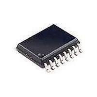
74HCT9046APW NXP Semiconductors, 74HCT9046APW Datasheet - Page 21

74HCT9046APW
Manufacturer Part Number
74HCT9046APW
Description
Phase Locked Loops (PLL) PLL BAND GAP CNTRL W/VCO
Manufacturer
NXP Semiconductors
Type
PLLr
Datasheet
1.74HCT9046AN112.pdf
(43 pages)
Specifications of 74HCT9046APW
Number Of Circuits
1
Supply Voltage (max)
5.5 V
Supply Voltage (min)
4.5 V
Maximum Operating Temperature
+ 125 C
Minimum Operating Temperature
- 40 C
Mounting Style
SMD/SMT
Operating Supply Voltage
4.5 V to 5.5 V
Package / Case
TSSOP-16
Lead Free Status / RoHS Status
Lead free / RoHS Compliant
Other names
74HCT9046APW,112
Available stocks
Company
Part Number
Manufacturer
Quantity
Price
Company:
Part Number:
74HCT9046APW
Manufacturer:
NXP
Quantity:
12 500
Company:
Part Number:
74HCT9046APW,118
Manufacturer:
CY
Quantity:
490
NXP Semiconductors
Table 6.
GND = 0 V; t
[1]
[2]
[3]
[4]
[5]
[6]
[7]
74HCT9046A_6
Product data sheet
Symbol
T
Phase comparator section
t
t
t
t
pd
en
dis
t
Fig 18. Waveforms showing input (SIG_IN and COMP_IN) to output (PCP_OUT and PC1_OUT) propagation
f/ T
amb
t
C
P
f
f
C
V
N = total load switching outputs;
Applies to the phase comparator section only (pin INH = HIGH). For power dissipation of the VCO and demodulator sections, see
Figure
This is the (peak to peak) input sensitivity.
This is the center frequency tolerance.
This is the frequency linearity.
This is the frequency stability with temperature change.
pd
i
o
D
CC
= 40 C to +125 C
PD
= input frequency in MHz;
L
(C
= output frequency in MHz;
is the same as t
= output load capacitance in pF;
= C
L
is used to determine the dynamic power dissipation (P
= supply voltage in V;
V
delays and the output transition times
PD
26,
V
M
Dynamic characteristics
CC
r
= 0.5V
= t
27
Parameter
frequency variation with
temperature
propagation delay
enable time
disable time
transition time
2
V
CC
f
and 28.
= 6 ns; C
f
o
2
) = sum of outputs.
CC
PLH
f
; V
i
I
N + (C
and t
= GND to V
L
= 50 pF.
PHL
PCP_OUT, PC1_OUT
L
; t
SIG_IN, COMP_IN
dis
V
outputs
CC
is the same as t
CC
inputs
.
[1]
2
…continued
f
o
) where:
Rev. 06 — 15 September 2009
Conditions
V
recommended range: R1 = 10 k ;
R2 = 10 k ; C1 = 1 nF; see
21
SIG_IN, COMP_IN to PC1_OUT;
V
SIG_IN, COMP_IN to PCP_OUT;
V
SIG_IN, COMP_IN to PC2_OUT;
V
SIG_IN, COMP_IN to PC2_OUT;
V
V
PLZ
CC
CC
CC
CC
CC
CC
and
and t
V
= 4.5 V; V
= 4.5 V; see
= 4.5 V; see
= 4.5 V; see
= 4.5 V; see
= 4.5 V; see
M
t
PHL
D
22
PHZ
in W).
; t
en
V
VCO_IN
M
is the same as t
t
Figure 18
Figure 18
Figure 19
Figure 19
Figure 18
THL
= 0.5V
CC
Figure
PZL
;
t
PLH
and t
PLL with band gap controlled VCO
20,
PZH
mbd106
; t
t
[7]
t
TLH
is the same as t
74HCT9046A
Min
-
-
-
-
-
-
Typ
0.06
-
-
-
-
-
© NXP B.V. 2009. All rights reserved.
TLH
and t
Max
-
60
102
84
98
22
THL
21 of 43
.
Unit
%/K
ns
ns
ns
ns
ns


