BCX55,115 NXP Semiconductors, BCX55,115 Datasheet
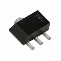
BCX55,115
Specifications of BCX55,115
BCX55 T/R
BCX55 T/R
Available stocks


Related parts for BCX55,115


BCX55,115 Summary of contents
Page 1
BC637; BCP55; BCX55 NPN medium power transistors Rev. 07 — 25 June 2007 1. Product profile 1.1 General description NPN medium power transistor series. Table 1. Type number [2] BC637 BCP55 BCX55 [1] Valid for all ...
Page 2
... NXP Semiconductors 2. Pinning information Table 3. Pin SOT54 SOT54A SOT54 variant SOT223 SOT89 BC637_BCP55_BCX55_7 Product data sheet Pinning Description base collector emitter base collector emitter base collector emitter base collector emitter collector emitter collector base Rev. 07 — 25 June 2007 BC637; BCP55; BCX55 NPN medium power transistors Simplifi ...
Page 3
... NXP Semiconductors 3. Ordering information Table 4. Type number [2] BC637 BCP55 BCX55 [1] Valid for all available selection groups. [2] Also available in SOT54A and SOT54 variant packages (see 4. Marking Table 5. Type number BC637 BC637-16 BCP55 BCP55-10 BCP55-16 BCX55 BCX55-10 BCX55-16 BC637_BCP55_BCX55_7 Product data sheet Ordering information ...
Page 4
... NXP Semiconductors 5. Limiting values Table 6. In accordance with the Absolute Maximum Rating System (IEC 60134). Symbol V CBO V CEO V EBO tot amb T stg [1] Device mounted on an FR4 Printed-Circuit Board (PCB), single-sided copper, tin-plated and standard footprint. [2] Device mounted on an FR4 PCB, single-sided copper, tin-plated, mounting pad for collector 1 cm ...
Page 5
... NXP Semiconductors 1.6 P tot (W) 1.2 0.8 0 FR4 PCB, standard footprint Fig 1. Power derating curve SOT54 (1) FR4 PCB, mounting pad for collector 6 cm (2) FR4 PCB, mounting pad for collector 1 cm (3) FR4 PCB, standard footprint Fig 3. Power derating curves SOT89 BC637_BCP55_BCX55_7 Product data sheet ...
Page 6
... NXP Semiconductors 6. Thermal characteristics Table 7. Symbol R th(j-a) R th(j-sp) [1] Device mounted on an FR4 PCB, single-sided copper, tin-plated and standard footprint. [2] Device mounted on an FR4 PCB, single-sided copper, tin-plated, mounting pad for collector 1 cm [3] Device mounted on an FR4 PCB, single-sided copper, tin-plated, mounting pad for collector 6 cm ...
Page 7
... NXP Semiconductors 3 10 duty cycle = Z th(j-a) (K/W) 1.0 0. 0.5 0.33 0.2 0.1 10 0.05 0.02 0. FR4 PCB, standard footprint Fig 5. Transient thermal impedance from junction to ambient as a function of pulse duration for SOT223; typical values th(j-a) (K/W) duty cycle = 0.75 0.5 0.33 0.2 ...
Page 8
... NXP Semiconductors 3 10 duty cycle = Z th(j-a) (K/W) 1.0 0.75 0 0.33 0.2 0.1 0.05 10 0.02 0. FR4 PCB, standard footprint Fig 7. Transient thermal impedance from junction to ambient as a function of pulse duration for SOT89; typical values th(j-a) (K/W) duty cycle = 0.75 0.5 0.33 0.2 ...
Page 9
... NXP Semiconductors 3 10 duty cycle = Z th(j-a) (K/W) 1 0.75 0.5 0.33 0.2 0.1 10 0.05 0.02 0. FR4 PCB, mounting pad for collector 6 cm Fig 9. Transient thermal impedance from junction to ambient as a function of pulse duration for SOT89; typical values 7. Characteristics Table unless otherwise specified. ...
Page 10
... NXP Semiconductors 300 h FE (1) 200 (2) 100 ( ( 150 C amb ( amb ( amb Fig 10. DC current gain as a function of collector current; typical values 1 (V) (1) 0.8 (2) 0 amb ( amb ( 150 C amb Fig 12. Base-emitter voltage as a function of collector current; typical values BC637_BCP55_BCX55_7 Product data sheet 006aaa080 ...
Page 11
... NXP Semiconductors 8. Package outline 4.2 3.6 4.8 4.4 5.2 14.5 5.0 12.7 Dimensions in mm Fig 14. Package outline SOT54 (SC-43A/TO-92) 4.2 3.6 2.5 max 4.8 4.4 5.2 14.5 5.0 12.7 Dimensions in mm Fig 16. Package outline SOT54 variant Fig 18. Package outline SOT89 (SC-62/TO-243) ...
Page 12
... NXP Semiconductors 9. Packing information Table 9. Packing methods The indicated -xxx are the last three digits of the 12NC ordering code. [2] Type number Package BC637 SOT54 SOT54A SOT54 variant BCP55 SOT223 BCX55 SOT89 [1] For further information and the availability of packing methods, see [2] Valid for all available selection groups. ...
Page 13
... Product data sheet Data sheet status Product data sheet The format of this data sheet has been redesigned to comply with the new identity guidelines of NXP Semiconductors. Legal texts have been adapted to the new company name where appropriate. Table 1 “Product overview”: amended Section 1.2 “ ...
Page 14
... For detailed and full information see the relevant full data sheet, which is available on request via the local NXP Semiconductors sales office. In case of any inconsistency or conflict with the short data sheet, the full data sheet shall prevail ...
Page 15
... NXP Semiconductors 13. Contents 1 Product profi 1.1 General description 1.2 Features . . . . . . . . . . . . . . . . . . . . . . . . . . . . . . 1 1.3 Applications . . . . . . . . . . . . . . . . . . . . . . . . . . . 1 1.4 Quick reference data Pinning information . . . . . . . . . . . . . . . . . . . . . . 2 3 Ordering information . . . . . . . . . . . . . . . . . . . . . 3 4 Marking . . . . . . . . . . . . . . . . . . . . . . . . . . . . . . . . 3 5 Limiting values Thermal characteristics Characteristics . . . . . . . . . . . . . . . . . . . . . . . . . . 9 8 Package outline . . . . . . . . . . . . . . . . . . . . . . . . 11 9 Packing information Revision history . . . . . . . . . . . . . . . . . . . . . . . . 13 11 Legal information ...