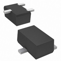
MSA1162GT1, MSA1162YT1
General Purpose Amplifier
Transistors
PNP Surface Mount
Features
•
•
•
Maximum ratings are those values beyond which device damage can occur.
Maximum ratings applied to the device are individual stress limit values (not
normal operating conditions) and are not valid simultaneously. If these limits are
exceeded, device functional operation is not implied, damage may occur and
reliability may be affected.
1. Pulse Test: Pulse Width ≤ 300 ms, D.C. ≤ 2%.
MAXIMUM RATINGS
© Semiconductor Components Industries, LLC, 2006
January, 2006 − Rev. 5
THERMAL CHARACTERISTICS
ELECTRICAL CHARACTERISTICS
Collector−Base Voltage
Collector−Emitter Voltage
Emitter−Base Voltage
Collector Current − Continuous
Collector Current − Peak
Power Dissipation
Junction Temperature
Storage Temperature
Collector−Emitter Breakdown Voltage
(I
Collector−Base Breakdown Voltage
(I
Emitter−Base Breakdown Voltage
(I
Collector−Base Cutoff Current
Collector−Emitter Cutoff Current
(V
(V
(V
DC Current Gain (Note 1)
(V
Collector−Emitter Saturation Voltage
(I
Current −Gain − Bandwidth Product
(I
C
C
E
C
C
Moisture Sensitivity Level: 1
ESD Rating: TBD
Pb−Free Packages are Available
CE
CE
CE
CE
= 10 mAdc, I
= 2.0 mAdc, I
= 10 mAdc, I
(V
= 100 mAdc, I
= 1 mA, V
= 10 Vdc, I
= 30 Vdc, I
= 30 Vdc, I
= 6.0 Vdc, I
CB
= 45 Vdc, I
Characteristic
Characteristic
CE
C
E
Rating
B
B
B
= 10.0 V, f = 10 MHz)
B
C
= 0)
= 0)
B
= 0)
= 0)
= 0, T
= 0)
= 2.0 mAdc)
= 10 mAdc)
E
= 0)
(T
A
MSA1162GT1
MSA1162YT1
A
= 80°C)
= 25°C)
(T
V
V
V
V
V
V
Symbol
Symbol
Symbol
V
(BR)CBO
(BR)CEO
(BR)EBO
A
(BR)CEO
(BR)CBO
(BR)EBO
I
I
CE(sat)
I
T
h
CBO
CEO
C(P)
P
T
= 25°C unless otherwise noted)
I
f
stg
FE
C
T
D
J
−55 to +150
Min
120
200
7.0
50
60
80
−
−
−
−
−
Value
Max
100
200
200
150
7.0
60
50
Max
240
400
0.1
0.1
2.0
1.0
0.5
−
−
−
−
1
mAdc
mAdc
mAdc
mAdc
mAdc
mAdc
MHz
Unit
Unit
Unit
Vdc
Vdc
Vdc
mW
Vdc
Vdc
Vdc
Vdc
°C
°C
−
*The “T1” suffix refers to a 7 inch reel.
†For information on tape and reel specifications,
MSA1162GT1
MSA1162GT1G
MSA1162YT1
MSA1162YT1G
including part orientation and tape sizes, please
refer to our Tape and Reel Packaging Specifications
Brochure, BRD8011/D.
Device*
*Date Code orientation may vary depending
(Note: Microdot may be in either location)
upon manufacturing location.
ORDERING INFORMATION
BASE
62x
M
G
MARKING DIAGRAM
2
http://onsemi.com
= Device Code
= Date Code*
= Pb−Free Package
(Pb−Free)
(Pb−Free)
Package
CASE 318D
x = G or Y
SC−59
SC−59
SC−59
SC−59
STYLE 1
62x M G
2
SC−59
COLLECTOR
G
Publication Order Number:
1
3
EMITTER
3
1
3000/Tape & Reel
3000/Tape & Reel
3000/Tape & Reel
3000/Tape & Reel
1
MSA1162GT1/D
Shipping
†


