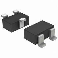
MMBT4401WT1G ON Semiconductor, MMBT4401WT1G Datasheet - Page 4

MMBT4401WT1G
Manufacturer Part Number
MMBT4401WT1G
Description
TRANS GP SS NPN 40V SOT323
Manufacturer
ON Semiconductor
Datasheet
1.MMBT4401WT1G.pdf
(6 pages)
Specifications of MMBT4401WT1G
Transistor Type
NPN
Current - Collector (ic) (max)
600mA
Voltage - Collector Emitter Breakdown (max)
40V
Vce Saturation (max) @ Ib, Ic
750mV @ 50mA, 500mA
Dc Current Gain (hfe) (min) @ Ic, Vce
100 @ 150mA, 1V
Power - Max
150mW
Frequency - Transition
250MHz
Mounting Type
Surface Mount
Package / Case
SC-70-3, SOT-323-3
Configuration
Single
Transistor Polarity
NPN
Mounting Style
SMD/SMT
Collector- Emitter Voltage Vceo Max
40 V
Emitter- Base Voltage Vebo
6 V
Continuous Collector Current
0.6 A
Maximum Dc Collector Current
0.6 A
Power Dissipation
150 mW
Maximum Operating Frequency
250 MHz
Maximum Operating Temperature
+ 150 C
Dc Collector/base Gain Hfe Min
20 at 0.1 mA at 1 V
Minimum Operating Temperature
- 55 C
Lead Free Status / RoHS Status
Lead free / RoHS Compliant
Current - Collector Cutoff (max)
-
Lead Free Status / Rohs Status
Lead free / RoHS Compliant
Other names
MMBT4401WT1GOS
Available stocks
Company
Part Number
Manufacturer
Quantity
Price
Company:
Part Number:
MMBT4401WT1G
Manufacturer:
ON Semiconductor
Quantity:
35 321
Company:
Part Number:
MMBT4401WT1G
Manufacturer:
ON
Quantity:
30 000
Part Number:
MMBT4401WT1G
Manufacturer:
ON/安森美
Quantity:
20 000
these curves, a high- - gain and a low- - gain unit were selected from the MMBT4401WT1 lines, and the same units were used
to develop the correspondingly numbered curves on each graph.
This group of graphs illustrates the relationship between h
300
200
100
8.0
6.0
4.0
2.0
7.0
5.0
3.0
2.0
1.0
0.7
0.5
0.3
0.2
70
50
30
20
10
10
0
0.01 0.02 0.05
0.1
0.1
0.2
0.2
Figure 13. Voltage Feedback Ratio
I
I
I
I
C
C
C
C
Figure 9. Frequency Effects
0.3
0.3
= 1.0 mA, R
= 500 mA, R
= 100 mA, R
= 50 mA, R
0.1
I
Figure 11. Current Gain
I
C
C
, COLLECTOR CURRENT (mA)
, COLLECTOR CURRENT (mA)
0.2
0.5 0.7 1.0
0.5 0.7 1.0
f, FREQUENCY (kHz)
S
0.5
S
S
S
= 4.0 kΩ
= 150 Ω
= 200 Ω
= 2.0 kΩ
1.0
SMALL- -SIGNAL CHARACTERISTICS
2.0 5.0
MMBT4401LT1 UNIT 1
MMBT4401LT1 UNIT 2
2.0 3.0
2.0
MMBT4401LT1 UNIT 1
MMBT4401LT1 UNIT 2
V
V
CE
R
RS =
RS =
CE
S
10
3.0
= OPTIMUM
= 10 Vdc, T
SOURCE
RESISTANCE
= 10 Vdc, f = 1.0 kHz, T
20
5.0 7.0
5.0 7.0
h PARAMETERS
http://onsemi.com
50
A
100
10
10
= 25C; Bandwidth = 1.0 Hz
fe
4
and other “h” parameters for this series of transistors. To obtain
6.0
4.0
2.0
8.0
10
5.0 k
2.0 k
1.0 k
0
50 k
20 k
10 k
500
100
50
5.0
2.0
1.0
50
10
20
0.1
0.1
100 200
A
Figure 10. Source Resistance Effects
f = 1.0 kHz
= 25C
0.2
0.2
NOISE FIGURE
I
I
I
I
C
C
C
C
R
Figure 14. Output Admittance
S
= 50 mA
= 100 mA
= 500 mA
= 1.0 mA
Figure 12. Input Impedance
, SOURCE RESISTANCE (OHMS)
0.3
0.3
500 1.0 k 2.0 k
I
I
C
C
, COLLECTOR CURRENT (mA)
, COLLECTOR CURRENT (mA)
0.5 0.7 1.0
0.5 0.7 1.0
5.0 k 10 k 20 k
MMBT4401LT1 UNIT 1
MMBT4401LT1 UNIT 2
2.0 3.0
2.0 3.0
MMBT4401LT1 UNIT 1
MMBT4401LT1 UNIT 2
50 k
5.0 7.0
5.0 7.0
100 k
10
10


