MMBTA56WT1G ON Semiconductor, MMBTA56WT1G Datasheet
MMBTA56WT1G
Specifications of MMBTA56WT1G
Available stocks


Related parts for MMBTA56WT1G


MMBTA56WT1G Summary of contents
Page 1
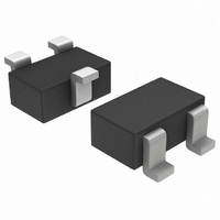
... Symbol Max Unit P 150 833 C/W θ +150 C J stg MMBTA56WT1G †For information on tape and reel specifications, including part orientation and tape sizes, please refer to our Tape and Reel Packaging Specifications Brochure, BRD8011/D. 1 http://onsemi.com COLLECTOR 3 1 BASE 2 EMITTER SC (SOT- - 323) ...
Page 2
ELECTRICAL CHARACTERISTICS Characteristic OFF CHARACTERISTICS Collector - - Emitter Breakdown Voltage (Note -1.0 mAdc Emitter - - Base Breakdown Voltage ( -100 mAdc Collector ...
Page 3
2 25C J 100 ...
Page 4
250 100 0 0 ...
Page 5
... A1 *For additional information on our Pb- -Free strategy and soldering details, please download the ON Semiconductor Soldering and Mounting Techniques Reference Manual, SOLDERRM/D. ON Semiconductor and are registered trademarks of Semiconductor Components Industries, LLC (SCILLC). SCILLC reserves the right to make changes without further notice to any products herein ...