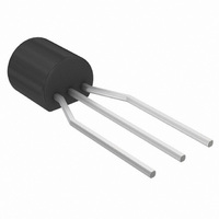
BC327-25RL1G ON Semiconductor, BC327-25RL1G Datasheet

TRANSISTOR PNP 45V 800MA TO-92

BC327-25RL1G

Manufacturer Part Number
BC327-25RL1G
Description
TRANSISTOR PNP 45V 800MA TO-92
Manufacturer
ON Semiconductor
Datasheet

Specifications of BC327-25RL1G

Transistor Type
PNP
Current - Collector (ic) (max)
800mA
Voltage - Collector Emitter Breakdown (max)
45V
Vce Saturation (max) @ Ib, Ic
700mV @ 50mA, 500mA
Current - Collector Cutoff (max)
100nA
Dc Current Gain (hfe) (min) @ Ic, Vce
160 @ 100mA, 1V
Power - Max
625mW
Frequency - Transition
260MHz
Mounting Type
Through Hole
Package / Case
TO-92-3 (Standard Body), TO-226
Lead Free Status / RoHS Status
Lead free / RoHS Compliant

Available stocks

Company
Part Number
Manufacturer
Quantity
Price
Part Number:
BC327-25RL1G
Manufacturer:
ON Semiconductor
Quantity:
5 350
Company:
Part Number:
BC327-25RL1G
Quantity:
7 800
BC327, BC327−16,
BC327−25, BC327−40
Amplifier Transistors
PNP Silicon
Features
Stresses exceeding Maximum Ratings may damage the device. Maximum
Ratings are stress ratings only. Functional operation above the Recommended
Operating Conditions is not implied. Extended exposure to stresses above the
Recommended Operating Conditions may affect device reliability.
*For additional information on our Pb−Free strategy and soldering details, please
© Semiconductor Components Industries, LLC, 2007
March, 2007 − Rev. 5
MAXIMUM RATINGS
THERMAL CHARACTERISTICS
download the ON Semiconductor Soldering and Mounting Techniques
Reference Manual, SOLDERRM/D.
Collector −Emitter Voltage
Collector −Base Voltage
Collector −Emitter Voltage
Collector Current − Continuous
Total Power Dissipation @ T
Operating and Storage Junction
Temperature Range
Thermal Resistance, Junction−to−Ambient
Thermal Resistance, Junction−to−Case
Pb−Free Packages are Available*
Derate above T
Derate above T
Characteristic
Rating
A
A
= 25°C
= 25°C
A
A
= 25°C
= 25°C
Symbol
Symbol
T
V
V
V
R
R
J
P
P
CEO
EBO
, T
CES
I
qJA
qJC
C
D
D
stg
−55 to +150
Value
−800
−5.0
Max
83.3
−45
−50
625
200
5.0
1.5
12
1
mW/°C
mW/°C
mAdc
°C/W
°C/W
Unit
Unit
Vdc
Vdc
Vdc
mW
°C
W
See detailed ordering, marking, and shipping information in
the package dimensions section on page 4 of this data sheet.
STYLE 17
CASE 29
TO−92
(Note: Microdot may be in either location)
ORDERING INFORMATION
BCxx = Device Code
A
Y
WW
G
STRAIGHT LEAD
BASE
MARKING DIAGRAM
http://onsemi.com
BULK PACK
2
1 2
= Assembly Location
= Year
= Work Week
= Pb−Free Package
3
COLLECTOR
AYWW G
EMITTER
BC
xx
Publication Order Number:
G
1
3
TAPE & REEL
AMMO PACK
BENT LEAD
1
2
3
BC327/D

Related parts for BC327-25RL1G

BC327-25RL1G Summary of contents

Page 1

... BC327, BC327−16, BC327−25, BC327−40 Amplifier Transistors PNP Silicon Features • Pb−Free Packages are Available* MAXIMUM RATINGS Rating Collector −Emitter Voltage Collector −Base Voltage Collector −Emitter Voltage Collector Current − Continuous Total Power Dissipation @ T = 25°C A Derate above T = 25°C ...

Page 2

... BC327, BC327−16, BC327−25, BC327−40 ELECTRICAL CHARACTERISTICS (T Characteristic OFF CHARACTERISTICS Collector −Emitter Breakdown Voltage (I = −10 mA Collector −Emitter Breakdown Voltage = −100 mA Emitter −Base Breakdown Voltage = −10 mA Collector Cutoff Current (V = − Collector Cutoff Current (V = − Emitter Cutoff Current (V = −4 CHARACTERISTICS DC Current Gain (I = − ...

Page 3

... BC327, BC327−16, BC327−25, BC327−40 −1000 1 25° −100 T = 25°C A CURRENT LIMIT THERMAL LIMIT SECOND BREAKDOWN LIMIT (APPLIES BELOW RATED V ) CEO −10 −1.0 −3.0 − COLLECTOR−EMITTER VOLTAGE CE Figure 2. Active Region − Safe Operating Area −1.0 −0.8 − ...

Page 4

... BC327, BC327−16, BC327−25, BC327−40 ORDERING INFORMATION Device Order Number Specific Device Marking BC327G BC327RL1G BC327−025G BC327−25RL1G BC327−25ZL1G BC327−40ZL1 BC327−40ZL1G †For information on tape and reel specifications, including part orientation and tape sizes, please refer to our Tape and Reel Packaging Specifications Brochure, BRD8011/D ...

Page 5

... BC327, BC327−16, BC327−25, BC327− SEATING PLANE SEATING K PLANE Semiconductor and are registered trademarks of Semiconductor Components Industries, LLC (SCILLC). SCILLC reserves the right to make changes without further notice to any products herein. SCILLC makes no warranty, representation or guarantee regarding the suitability of its products for any particular purpose, nor does SCILLC assume any liability arising out of the application or use of any product or circuit, and specifically disclaims any and all liability, including without limitation special, consequential or incidental damages. “ ...

Related keywords