BSP52T3G ON Semiconductor, BSP52T3G Datasheet

TRANS DARL NPN 80V 1A SOT-223

BSP52T3G

Manufacturer Part Number
BSP52T3G
Description
TRANS DARL NPN 80V 1A SOT-223
Manufacturer
ON Semiconductor
Datasheet

Specifications of BSP52T3G

Transistor Type
NPN - Darlington
Current - Collector (ic) (max)
1A
Voltage - Collector Emitter Breakdown (max)
80V
Vce Saturation (max) @ Ib, Ic
1.3V @ 500µA, 500mA
Current - Collector Cutoff (max)
10µA
Dc Current Gain (hfe) (min) @ Ic, Vce
2000 @ 500mA, 10V
Power - Max
800mW
Mounting Type
Surface Mount
Package / Case
SOT-223 (3 leads + Tab), SC-73, TO-261
Polarity
NPN
Number Of Elements
1
Collector-emitter Voltage
80V
Collector-base Voltage
90V
Emitter-base Voltage
5V
Base-emitter Saturation Voltage (max)
1.9@0.5mA@500mAV
Collector-emitter Saturation Voltage
1.3@0.5mA@500mAV
Collector Current (dc) (max)
1A
Operating Temp Range
-65C to 150C
Operating Temperature Classification
Military
Mounting
Surface Mount
Pin Count
3 +Tab
Package Type
SOT-223
Lead Free Status / RoHS Status
Lead free / RoHS Compliant
Frequency - Transition
-
Lead Free Status / Rohs Status
Compliant

Available stocks

Company
Part Number
Manufacturer
Quantity
Price
Part Number:
BSP52T3G
Manufacturer:
ON
Quantity:
12 500
BSP52T1G, BSP52T3G
NPN Small-Signal
Darlington Transistor
switching applications, such as print hammer, relay, solenoid and lamp
drivers. The device is housed in the SOT-223 package, which is
designed for medium power surface mount applications.
Features
Stresses exceeding Maximum Ratings may damage the device. Maximum
Ratings are stress ratings only. Functional operation above the Recommended
Operating Conditions is not implied. Extended exposure to stresses above the
Recommended Operating Conditions may affect device reliability.
1. Device mounted on a FR-4 glass epoxy printed circuit board using minimum
2. Device mounted on a FR-4 glass epoxy printed circuit board using 1 cm
THERMAL CHARACTERISTICS
© Semiconductor Components Industries, LLC, 2010
September, 2010 − Rev. 6
MAXIMUM RATINGS
Collector-Emitter Voltage
Collector-Base Voltage
Emitter-Base Voltage
Collector Current
Total Power Dissipation (Note 1)
Total Power Dissipation (Note 2)
Operating and Storage
Thermal Resistance (Note 1)
Thermal Resistance (Note 2)
Maximum Temperature for Soldering
This NPN small signal Darlington transistor is designed for use in
formed leads absorb thermal stress during soldering, eliminating the
possibility of damage to the die
Use BSP52T1 to Order the 7 Inch/1000 Unit Reel
Compliant
The SOT-223 Package can be soldered using wave or reflow. The
Available in 12 mm Tape and Reel
PNP Complement is BSP62T1
These Devices are Pb−Free, Halogen Free/BFR Free and are RoHS
recommended footprint.
@ T
Derate above 25°C
@ T
Derate above 25°C
Temperature Range
Junction-to-Ambient
Junction-to-Ambient
Purposes
Time in Solder Bath
A
A
= 25°C
= 25°C
Characteristic
Rating
(T
C
= 25°C unless otherwise noted)
Symbol
Symbol
T
V
V
V
R
R
J
P
P
CES
CBO
EBO
, T
T
I
qJA
qJA
C
D
D
L
stg
−65 to 150
Value
Max
1.25
156
100
260
5.0
1.0
0.8
6.4
80
90
10
10
1
mW/°C
mW/°C
°C/W
°C/W
Unit
Unit
Vdc
Vdc
Vdc
Adc
Sec
°C
°C
W
W
2
pad.
†For information on tape and reel specifications,
BSP52T1G
BSP52T3G
including part orientation and tape sizes, please
refer to our Tape and Reel Packaging Specifications
Brochure, BRD8011/D.
DARLINGTON TRANSISTOR
Device
CASE 318E
1
SOT−223
STYLE 1
A
Y
W
AS3
G
(Note: Microdot may be in either location)
2
ORDERING INFORMATION
SURFACE MOUNT
3
MEDIUM POWER
http://onsemi.com
NPN SILICON
= Assembly Location
= Year
= Work Week
= Specific Device Code
= Pb−Free Package
4
(Pb−Free)
(Pb−Free)
SOT−223
SOT−223
Package
BASE
1
COLLECTOR 2,4
EMITTER 3
Publication Order Number:
MARKING DIAGRAM
1000/Tape & Reel
4000/Tape & Reel
Shipping
AS3G
AYW
G
BSP52T1/D

Related parts for BSP52T3G

BSP52T3G Summary of contents

Page 1

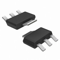
... BSP52T1G, BSP52T3G NPN Small-Signal Darlington Transistor This NPN small signal Darlington transistor is designed for use in switching applications, such as print hammer, relay, solenoid and lamp drivers. The device is housed in the SOT-223 package, which is designed for medium power surface mount applications. Features • ...

Page 2

ELECTRICAL CHARACTERISTICS Characteristics OFF CHARACTERISTICS Collector-Base Breakdown Voltage (I = 100 mAdc Emitter-Base Breakdown Voltage ( mAdc Collector-Emitter Cutoff Current ( Vdc ...

Page 3

... A1 *For additional information on our Pb−Free strategy and soldering details, please download the ON Semiconductor Soldering and Mounting Techniques Reference Manual, SOLDERRM/D. ON Semiconductor and are registered trademarks of Semiconductor Components Industries, LLC (SCILLC). SCILLC reserves the right to make changes without further notice to any products herein ...

Related keywords