Standard Resistance Range
Total Resistance Tolerance
Standard Tapers ................Linear & audio
Maximum Operating Voltage
Rated Power
Noise .................................. 100 mV max.
Insulation Resistance @ 250 VDC
Dielectric Withstanding Voltage
End Resistance .................20 ohms max.
Tracking Error (-40 dB to 0 dB) .......±3 dB
Operating Temperature
Rotational Life ................... 15,000 cycles
IP Rating .......................................... IP 40
Mechanical Angle ...................300 ° ±10 °
Running Torque ...............10 to 250 g-cm
Stop Strength .......................... 4.0 kg-cm
Shaft Push/Pull Strength .......5.0 kgf min.
Shaft Wobble .....0.6 x L/20 mm p-p max.
Mounting Torque ............. 7.0 kg-cm min.
Soldering Condition
Mounting Hardware ........ One fl at washer
Electrical Characteristics
Environmental Characteristics
Mechanical Characteristics
Derating Curve
Linear Taper .......................0.05 watts
Audio Taper ......................0.025 watts
Manual Soldering
Wave Soldering
Wash Process ...... Not recommended
....................... 1 K ohms to 1 M ohms
.................................±10 % or ±20 %
............................... 150 VAC, 20 VDC
....................................... 100 M ohms
..............................................300 VAC
.................................-10 °C to +50 °C
........96.5 Sn/3.0 Ag/0.5 Cu solid wire
............. 96.5 Sn/3.0 Ag/0.5 Cu solder
100
80
60
40
33
20
0
0
10
and one mounting nut supplied
20
Ambient Temperature (°C)
or no-clean rosin cored wire
270 °C max. for 3 seconds
260 °C max. for 5 seconds
30
40 50 60 70 80 90 100
per potentiometer
with no-clean fl ux
Features
■
■
■
■
■
■
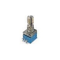
PTD90 Series - 9 mm Multi-Ganged Potentiometer
RECOMMENDED PCB LAYOUT
SCHEMATIC
PTD901
(.039 +.008/-0)
Product Dimensions
Carbon element
Ganging up to 8 sections available
Knurled and fl atted shaft styles
Audio taper option
Tracking error within 3 dB
RoHS compliant*
DIA. HOLES
1.0 +0.2/-0
3 PLCS.
R1
R1
(.197)
1
5.0
(.278 ± .020)
(.197)
7.05 ± 0.5
5.0
(.014 ± .007)
R1
0.8 ± 0.2
M7XP0.75
3
2
1
2
(.197)
5.0
3
MOUNTING
Customers should verify actual device performance in their specifi c applications.
SURFACE
*RoHS Directive 2002/95/EC Jan 27 2003 including Annex
RECOMMENDED PCB LAYOUT
PTD902
SCHEMATIC
(.039 +.008/-0)
DIA. HOLES
1.0 +0.2/-0
Specifi cations are subject to change without notice.
6 PLCS.
R2
DIMENSIONS:
R1
R2
(.380 ± .020)
(.197)
9.65 ± 0.5
5.0
1'
1
R1
(.098)
2.5
R2
3
2
1
R1
2'
2
(INCHES)
(.197)
3
2
1
5.0
(.014 ± .007)
(.098)
MM
2.5
0.8 ± 0.2
M7XP0.75
(.197)
5.0
3'
3
MOUNTING
SURFACE