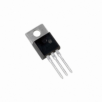
TIP115G ON Semiconductor, TIP115G Datasheet - Page 7

TIP115G
Manufacturer Part Number
TIP115G
Description
TRANS DARL PNP 2A 60V TO220AB
Manufacturer
ON Semiconductor
Type
Medium Power, Switchr
Specifications of TIP115G
Transistor Type
PNP - Darlington
Current - Collector (ic) (max)
2A
Voltage - Collector Emitter Breakdown (max)
60V
Vce Saturation (max) @ Ib, Ic
2.5V @ 8mA, 2A
Current - Collector Cutoff (max)
2mA
Dc Current Gain (hfe) (min) @ Ic, Vce
1000 @ 1A, 4V
Power - Max
2W
Mounting Type
Through Hole
Package / Case
TO-220-3 (Straight Leads)
Current, Gain
500
Current, Input
50 mA
Current, Output
2 A
Package Type
TO-220AB
Polarity
PNP
Power Dissipation
50 W
Primary Type
Si
Resistance, Thermal, Junction To Ambient
62.5
Voltage, Collector To Emitter, Saturation
2.5 V
Voltage, Input
5 V
Voltage, Output
60 V
Lead Free Status / RoHS Status
Lead free / RoHS Compliant
Frequency - Transition
-
Lead Free Status / Rohs Status
RoHS Compliant part
Electrostatic Device
Other names
TIP115GOS
INPUT
+ 0.8
- 0.8
- 1.6
- 4.0
- 4.8
10
- 2.4
- 3.2
V
10
10
10
10
10
10
-1
BB1
0.04 0.06
0
5
4
3
2
1
0
- 0.6
50 W
Note A: Input pulse width is increased until I
NPN test shown; for PNP test
reverse all polarity and use MJE224 driver.
= 10 V
T
100°C
J
REVERSE
- 0.4 - 0.2
25°C
q
V
*APPLIES FOR I
= 150°C
MJE254
CE
* q
VC
50 W
VC
for V
= 30 V
0.1
for V
V
BE
BE
+
-
I
C
, BASE‐EMITTER VOLTAGE (VOLTS)
CE(sat)
TIP110, TIP111, TIP112 (NPN); TIP115, TIP116, TIP117 (PNP)
, COLLECTOR CURRENT (AMP)
0
100 W
2 kW
R
R
C
0.2
BB1
/I
BB2
TIP110, 111, 112
TEST CIRCUIT
B
+ 0.2 + 0.4 + 0.6 + 0.8 + 1.0 + 1.2
FORWARD
≤ h
FE
V
NPN
/3
BB2
0.4 0.6
25°C to 150°C
= 0
25°C to 150°C
- 55°C to 25°C
- 55°C to 25°C
1.0
Figure 13. Inductive Load Switching
Figure 11. Temperature Coefficients
Figure 12. Collector Cut‐Off Region
0.1 W
V
TUT
CM
R
CE
S
=
MONITOR
= 0.71 A,
2.0
-
+
100 mH
V
http://onsemi.com
CC
= 20 V
+ 1.4
MONITOR
4.0
I
C
7
10
+ 0.8
- 0.8
- 1.6
- 2.4
- 3.2
- 4.0
- 4.8
10
10
10
10
10
10
COLLECTOR
COLLECTOR
-1
CURRENT
0.04 0.06
VOLTAGE
VOLTAGE
0
5
4
3
2
1
0
- 0.6
INPUT
T
*APPLIES FOR I
J
- 0.4 - 0.2
REVERSE
q
100°C
V
= 150°C
VC
* q
CE
VOLTAGE AND CURRENT WAVEFORMS
V
VC
for V
25°C
0.71 A
= 30 V
CE(sat)
V
20 V
0.1
- 5 V
for V
CER
0 V
0 V
V
BE
BE
I
CE(sat)
C
, BASE‐EMITTER VOLTAGE (VOLTS)
, COLLECTOR CURRENT (AMP)
C
0
/I
B
0.2
TIP115, 116, 117
≤ h
+ 0.2 + 0.4 + 0.6 + 0.8 + 1.0 + 1.2
FORWARD
FE
/3
PNP
25°C to 150°C
100 ms
0.4 0.6
t
w
- 55°C to 25°C
≈ 3.5 ms (SEE NOTE A)
25°C to 150°C
- 55°C to 25°C
1.0
2.0
+ 1.4
4.0


