MJE210G ON Semiconductor, MJE210G Datasheet

TRANS PWR PNP 5A 25V TO225AA

MJE210G

Manufacturer Part Number
MJE210G
Description
TRANS PWR PNP 5A 25V TO225AA
Manufacturer
ON Semiconductor
Type
Powerr
Datasheets

Specifications of MJE210G

Transistor Type
PNP
Current - Collector (ic) (max)
5A
Voltage - Collector Emitter Breakdown (max)
40V
Vce Saturation (max) @ Ib, Ic
1.8V @ 1A, 5A
Dc Current Gain (hfe) (min) @ Ic, Vce
45 @ 2A, 1V
Power - Max
15W
Frequency - Transition
65MHz
Mounting Type
Through Hole
Package / Case
TO-225-3
Transistor Polarity
PNP
Mounting Style
Through Hole
Collector- Emitter Voltage Vceo Max
40 V
Emitter- Base Voltage Vebo
8 V
Maximum Dc Collector Current
5 A
Power Dissipation
15 W
Maximum Operating Temperature
+ 150 C
Continuous Collector Current
5 A
Dc Collector/base Gain Hfe Min
70
Maximum Operating Frequency
65 MHz
Minimum Operating Temperature
- 65 C
Current, Collector
5 A
Current, Gain
10
Frequency
65 MHz
Package Type
TO-225
Polarity
PNP
Primary Type
Si
Resistance, Thermal, Junction To Case
8.34 °C/W
Voltage, Breakdown, Collector To Emitter
40 V
Voltage, Collector To Base
25 V
Voltage, Collector To Emitter
40 V
Voltage, Collector To Emitter, Saturation
1.8 V
Voltage, Emitter To Base
8 V
Number Of Elements
1
Collector-emitter Voltage
25V
Collector-base Voltage
40V
Emitter-base Voltage
8V
Collector Current (dc) (max)
5A
Dc Current Gain (min)
70
Frequency (max)
65MHz
Operating Temp Range
-65C to 150C
Operating Temperature Classification
Military
Mounting
Through Hole
Pin Count
3 +Tab
Lead Free Status / RoHS Status
Lead free / RoHS Compliant
Current - Collector Cutoff (max)
-
Lead Free Status / Rohs Status
Lead free / RoHS Compliant
Other names
MJE210GOS

Available stocks

Company
Part Number
Manufacturer
Quantity
Price
Part Number:
MJE210G
Manufacturer:
ON/安森美
Quantity:
20 000
Company:
Part Number:
MJE210G
Quantity:
200
MJE200 - NPN,
MJE210 - PNP
Complementary Silicon
Power Plastic Transistors
audio amplifier applications.
Features
Stresses exceeding Maximum Ratings may damage the device. Maximum
Ratings are stress ratings only. Functional operation above the Recommended
Operating Conditions is not implied. Extended exposure to stresses above the
Recommended Operating Conditions may affect device reliability.
*For additional information on our Pb-Free strategy and soldering details, please
© Semiconductor Components Industries, LLC, 2007
July, 2007 - Rev. 12
MAXIMUM RATINGS
THERMAL CHARACTERISTICS
download the ON Semiconductor Soldering and Mounting Techniques
Reference Manual, SOLDERRM/D.
Collector-Emitter Voltage
Collector-Base Voltage
Emitter-Base Voltage
Collector Current
Base Current
Total Power Dissipation @ T
Operating and Storage Junction
Temperature Range
Thermal Resistance, Junction-to-Case
Thermal Resistance,
These devices are designed for low voltage, low-power, high-gain
Collector-Emitter Sustaining Voltage -
High DC Current Gain -
Low Collector-Emitter Saturation Voltage -
High Current-Gain - Bandwidth Product -
Annular Construction for Low Leakage -
Pb-Free Packages are Available*
Derate above 25_C
Derate above 25_C
Junction-to-Ambient
V
h
V
f
I
T
CBO
Characteristic
FE
CEO(sus)
CE(sat)
= 65 MHz (Min) @ I
= 100 mAdc
= 70 (Min) @ I
= 45 (Min) @ I
= 10 (Min) @ I
Rating
= 100 nAdc @ Rated V
- Continuous
- Peak
= 0.3 Vdc (Max) @ I
= 0.75 Vdc (Max) @ I
= 25 Vdc (Min) @ I
C
C
Preferred Device
= 25_C
= 25_C
C
C
C
= 500 mAdc
= 2.0 Adc
= 5.0 Adc
C
Symbol
Symbol
T
CB
V
C
J
V
V
q
q
P
P
C
CEO
, T
I
I
C
CB
EB
JC
JC
C
B
= 500 mAdc
D
D
= 10 mAdc
stg
= 2.0 Adc
–65 to +150
Value
0.012
0.12
Max
8.34
83.4
8.0
5.0
1.0
1.5
40
25
10
15
1
mW/_C
mW/_C
_C/W
_C/W
Unit
Unit
Vdc
Vdc
Vdc
Adc
Adc
_C
W
W
Preferred devices are recommended choices for future use
and best overall value.
MJE200
MJE200G
MJE210
MJE210G
MJE210T
MJE210TG
COMPLEMENTARY SILICON
Device
POWER TRANSISTORS
3
25 VOLTS, 15 WATTS
ORDERING INFORMATION
2 1
Y
WW
JE2x0 = Device Code
G
MARKING DIAGRAM
5.0 AMPERES
http://onsemi.com
(Pb-Free)
(Pb-Free)
(Pb-Free)
= Year
= Work Week
= Pb-Free Package
Package
TO-225
TO-225
TO-225
TO-225
TO-225
TO-225
x = 0 or 1
Publication Order Number:
JE2x0G
YWW
CASE 77
STYLE 1
TO-225
500 Units/Box
500 Units/Box
500 Units/Box
500 Units/Box
50 Units/Rail
50 Units/Rail
Shipping
MJE200/D

Related parts for MJE210G

MJE210G Summary of contents

Page 1

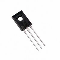
... J stg MJE200 MJE200G Symbol Max Unit q _C/W 8. _C/W MJE210 83.4 JC MJE210G MJE210T MJE210TG Preferred devices are recommended choices for future use and best overall value. 1 http://onsemi.com 5.0 AMPERES POWER TRANSISTORS COMPLEMENTARY SILICON 25 VOLTS, 15 WATTS TO-225 CASE 77 STYLE MARKING DIAGRAM ...

Page 2

ELECTRICAL CHARACTERISTICS Î Î Î Î Î ...

Page 3

MJE200 - NPN + 9.0 V ≤ DUTY CYCLE = 1.0% R and R VARIED TO OBTAIN DESIRED CURRENT LEVELS B C ...

Page 4

MJE200 - NPN, 10 7.0 1.0 ms 5.0 3.0 dc 5 150°C 1.0 J BONDING WIRE LIMITED 0.7 THERMALLY LIMITED @ T = 25°C 0.5 C (SINGLE PULSE) 0.3 SECOND BREAKDOWN LIMITED CURVES APPLY BELOW 0.2 ...

Page 5

MJE200 - NPN, NPN MJE200 400 T = 150°C J 25°C 200 - 55°C 100 1 2 0.05 0.07 0.1 0.2 0.3 0.5 0.7 1 COLLECTOR ...

Page 6

... Opportunity/Affirmative Action Employer. This literature is subject to all applicable copyright laws and is not for resale in any manner. PUBLICATION ORDERING INFORMATION LITERATURE FULFILLMENT:  Literature Distribution Center for ON Semiconductor  P.O. Box 5163, Denver, Colorado 80217 USA  Phone: 303-675-2175 or 800-344-3860 Toll Free USA/Canada  Fax: 303-675-2176 or 800-344-3867 Toll Free USA/Canada   ...

Related keywords