2N6039G ON Semiconductor, 2N6039G Datasheet
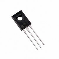
TRANS DARL NPN 4A 80V TO225AA

2N6039G

Manufacturer Part Number
2N6039G
Description
TRANS DARL NPN 4A 80V TO225AA
Manufacturer
ON Semiconductor
Type
Power, Switchr
Datasheets

Specifications of 2N6039G

Transistor Type
NPN - Darlington
Current - Collector (ic) (max)
4A
Voltage - Collector Emitter Breakdown (max)
80V
Vce Saturation (max) @ Ib, Ic
3V @ 40mA, 4A
Current - Collector Cutoff (max)
100µA
Dc Current Gain (hfe) (min) @ Ic, Vce
750 @ 2A, 3V
Power - Max
40W
Mounting Type
Through Hole
Package / Case
TO-225-3
Polarity
NPN
Number Of Elements
1
Collector-emitter Voltage
80V
Collector-base Voltage(max)
80V
Emitter-base Voltage (max)
5V
Base-emitter Saturation Voltage (max)
4@40mA@4AV
Collector-emitter Saturation Voltage
2@8mA@2A/3@40mA@4AV
Collector Current (dc) (max)
4A
Operating Temp Range
-65C to 150C
Operating Temperature Classification
Military
Mounting
Through Hole
Pin Count
3 +Tab
Package Type
TO-225
Configuration
Single
Transistor Polarity
NPN
Mounting Style
SMD/SMT
Collector- Emitter Voltage Vceo Max
80 V
Emitter- Base Voltage Vebo
5 V
Collector- Base Voltage Vcbo
80 V
Maximum Dc Collector Current
4 A
Maximum Collector Cut-off Current
500 uA
Power Dissipation
40 W
Maximum Operating Temperature
+ 150 C
Continuous Collector Current
4 A
Dc Collector/base Gain Hfe Min
100, 500, 750
Minimum Operating Temperature
- 65 C
Current, Gain
100
Current, Input
100 mA
Current, Output
4 A
Primary Type
Si
Resistance, Thermal, Junction To Ambient
83.3
Voltage, Collector To Emitter, Saturation
3 V
Voltage, Input
5 V
Voltage, Output
80 V
Lead Free Status / RoHS Status
Lead free / RoHS Compliant
Frequency - Transition
-
Lead Free Status / Rohs Status
Compliant
Other names
2N6039GOS

Available stocks

Company
Part Number
Manufacturer
Quantity
Price
Part Number:
2N6039G
Manufacturer:
ON
Quantity:
500
(PNP) 2N6034, 2N6035,
2N6036; (NPN) 2N6038,
2N6039
Plastic Darlington
Complementary Silicon
Power Transistors
designed for general purpose amplifier and low−speed switching
applications.
Features
Stresses exceeding Maximum Ratings may damage the device. Maximum
Ratings are stress ratings only. Functional operation above the Recommended
Operating Conditions is not implied. Extended exposure to stresses above the
Recommended Operating Conditions may affect device reliability.
*For additional information on our Pb−Free strategy and soldering details, please
MAXIMUM RATINGS
THERMAL CHARACTERISTICS
download the ON Semiconductor Soldering and Mounting Techniques
Reference Manual, SOLDERRM/D.
Collector−Emitter Voltage
Collector−Base Voltage
Emitter−Base Voltage
Collector Current
Base Current
Total Device Dissipation @ T
Operating and Storage Junction
Temperature Range
Thermal Resistance, Junction−to−Case
Thermal Resistance, Junction−to−Ambient
Plastic Darlington complementary silicon power transistors are
Derate above 25°C
Derate above 25°C
ESD Ratings: Machine Model, C; > 400 V
Epoxy Meets UL 94 V−0 @ 0.125 in
Pb−Free Packages are Available*
Characteristic
Human Body Model, 3B; > 8000 V
Rating
2N6035, 2N6038
2N6036, 2N6039
2N6035, 2N6038
2N6036, 2N6039
C
C
= 25°C
= 25°C
Continuous
2N6034
2N6034
Peak
Symbol
Symbol
T
V
V
V
R
R
J
P
P
CEO
CBO
EBO
, T
I
I
qJC
qJA
C
B
D
D
stg
– 65 to
Value
+ 150
Max
3.12
83.3
100
320
5.0
4.0
8.0
1.5
40
60
80
40
60
80
40
12
1
mW/°C
mW/°C
mAdc
°C/W
°C/W
Unit
Unit
Vdc
Vdc
Vdc
Adc
Apk
°C
W
W
See detailed ordering and shipping information in the package
dimensions section on page 5 of this data sheet.
4.0 AMPERES DARLINGTON
COMPLEMENTARY SILICON
40, 60, 80 VOLTS, 40 WATTS
POWER TRANSISTORS
3 2
ORDERING INFORMATION
Y
WW
2N603x = Device Code
G
1
MARKING DIAGRAM
BASE
3
COLLECTOR 2,4
= Year
= Work Week
= Pb−Free Package
x = 4, 5, 6, 8, 9
EMITTER 1
N603xG
YWW
TO−225AA
CASE 77
STYLE 1
2

Related parts for 2N6039G

2N6039G Summary of contents

Page 1

... Ratings are stress ratings only. Functional operation above the Recommended Operating Conditions is not implied. Extended exposure to stresses above the Recommended Operating Conditions may affect device reliability. *For additional information on our Pb−Free strategy and soldering details, please download the ON Semiconductor Soldering and Mounting Techniques Reference Manual, SOLDERRM/D. Symbol Value ...

Page 2

ELECTRICAL CHARACTERISTICS Characteristic OFF CHARACTERISTICS Collector−Emitter Sustaining Voltage (I = 100 mAdc Collector−Cutoff Current ( Vdc Vdc ...

Page 3

... C B 0.6 0.2 0.04 0.06 0.1 0.2 0.4 0 COLLECTOR CURRENT (AMP) C ORDERING INFORMATION Device 2N6034 2N6034G 2N6035 2N6035G 2N6036 2N6036G 2N6038 2N6038G 2N6039 2N6039G 3 25° 0.5 A 2.6 4.0 A 2.2 1.8 1.4 1.0 0 100 0.1 0.2 Figure 8. Collector Saturation Region 2 ...

Page 4

−A− 0.25 (0.010 0.25 (0.010 PACKAGE DIMENSIONS TO−225AA CASE 77−09 ISSUE Z NOTES: 1. DIMENSIONING AND ...

Related keywords