AD9959/PCB Analog Devices Inc, AD9959/PCB Datasheet
AD9959/PCB
Specifications of AD9959/PCB


AD9959/PCB Summary of contents
Page 1
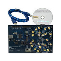
... This document is intended for use in conjunction with the AD9959 data sheet, which is available from Analog Devices at www.analog.com. One Technology Way, P.O. Box 9106, Norwood, MA 02062-9106, U.S.A. Tel: 781.329.4700 Fax: 781.461.3113 Evaluation Board for AD9959/PCB J2 DAC 0 OUT J6 DAC 0 FILTER OUT DAC 0 IOUT LPF ...
Page 2
... AD9959/PCB TABLE OF CONTENTS Evaluation Board Block Diagram................................................... 1 Features .............................................................................................. 1 Applications....................................................................................... 1 General Description ......................................................................... 1 Evaluation Board Hardware ............................................................ 3 Package Contents.......................................................................... 3 Requirements ................................................................................ 3 Setting up the Evaluation Board................................................. 3 Powering the Part ..................................................................... 3 Clocking the Part...................................................................... 3 Communicating with the Part................................................ 3 Evaluation Board Layout ............................................................. 4 Evaluation Board Software .............................................................. 5 Installing the Software ................................................................. 5 Configuring the Evaluation Board............................................. 5 Windows 98/ME/2000 Users ...
Page 3
... J17 J18 J19 J20 Note that the AD9959/PCB is preconfigured so that the CLK_VDD, BG_VDD, and all other AVDD connections are tied together. Therefore, only one connection (J10, J16, J17, J18, J19, or J20) needs power for proper functionality of all four channels. These AVDD connections can be separated for better channel isolation. This is accomplished by removing the 0 Ω ...
Page 4
... AD9959/PCB MANUAL I/O CONTROL HEADERS EVALUATION BOARD CONTROL USB PORT SDIO Manual I/O Control Headers Provides the interface for communication with the AD9959 when the part is under the control of an external controller (manual control). See Eval Board Control for correct jumper settings ...
Page 5
... If you are using Windows 2000, click Finish if you see this window (Figure 5). 6. Next, the window in Figure 6 appears. After the window has disappeared, the USB Status LED (CR2 on AD9959 evaluation board) flashes, which indicates that the evaluation board is connected properly. Rev Page AD9959/PCB Figure 4. Figure 5. Figure 6. ...
Page 6
... AD9959/PCB Windows XP Users 1. Power up the AD9959 evaluation board (see Table 2). 2. Connect the evaluation board to the computer using a USB cable via the USB port. Then, the VBUS LED (CR1 on AD9959 evaluation board) illuminates. 3. When the USB cable is connected, the screen below appears (Figure 7) ...
Page 7
... Figure 13). After completing these steps, the AD9959 evaluation software loads onto your PC system. You are then presented with one of several status messages. These messages are discussed in further detail in the next section, Status Messages upon Loading Software. Rev Page AD9959/PCB Figure 13. ...
Page 8
... AD9959/PCB Status Messages upon Loading Software Once the AD9959 evaluation software has been loaded, a green splash screen appears as shown in Figure 14. The status box within the splash screen gives the status of the AD9959 evaluation software. A cursor is provided for easy navigation throughout this box. Green writing in the status box indicates that the software has successfully loaded ...
Page 9
... Multiplier selects the PLL multiplication factor (4× to 20×) by which to scale the input frequency. The default setting of this box is Disabled, indicating that the Ref Clock Multiplier circuitry is bypassed and the Ref Clock/Crystal input is piped directly to the DDS core. Rev Page AD9959/PCB Figure 19. ...
Page 10
... AD9959/PCB CP Current selects the charge pump current output of the PLL in the Ref Clock Multiplier circuitry. Selecting a higher current output will result in the loop locking faster, but there is a trade-off. Increasing this current output will also increase phase noise. The default setting of this box is 75 μA. ...
Page 11
... Latency Control section, the pipeline delay for updates to frequency, amplitude, and phase will be equal, but only for the channels operating in single tone mode. The default setting of this box is unchecked, meaning the pipeline delay for updates to frequency, amplitude, and phase will not be equal. Rev Page AD9959/PCB Figure 22. ...
Page 12
... AD9959/PCB See the DATA LATENCY (PIPELINE DELAY) section in the Specifications table of the AD9959 data sheet for the exact timing delays with and without this feature enabled. Also, refer to the Single Tone Mode-Matched Pipeline Delay section of the AD9959 data sheet. 6. DAC Full Scale Current Control Use the DAC Full Scale Current Control section to scale the output current of the DAC ...
Page 13
... The value of .00098 is derived from this equation: IntegerFac tor In the second box, set the desired output amplitude scale factor (between 0 and 1) of the output signal, where 1 is equivalent to full scale. Rev Page AD9959/PCB × × ° ...
Page 14
... AD9959/PCB The Enable ASF box also represents the starting point of the linear amplitude sweep and the first level in amplitude modulation (ASK). Note that when performing linear amplitude sweeps, the Enable ASF box must be left unchecked. When using the RU/RD feature, the Enable Auto ASF box must be checked ...
Page 15
... Channel 0. To access the internal registers of the selected channel, use the RegAddr drop menu to select which register(s) you would like to read/write. You can also directly toggle the states of any external input pins such as the profile or SDIO data pins. Rev Page AD9959/PCB ...
Page 16
... AD9959/PCB Figure 30. To access the Debug Window, click View and select Debug Window (see Figure 31). Figure 31. DUT I/O Box This dialog box (Figure 32) controls the I/O configuration for the device. Click I/O Reset to send an I/O reset to the corresponding serial port state machine. Select LSB First to change the data format to LSB first from the default setting of MSB first ...
Page 17
... To load these setup files click File, and select Load Setup… (Figure 33), or click the open folder (Figure 34) to access these files. Figure 33. Next, open the AD9959 Configuration Files folder (Figure 35). Then select which mode of operation setup file(s) you would like to view (see Figure 36). Select Linear Sweep Mode, Modulation Mode, or Single Tone Mode. Figure 35. Figure 36. Rev Page AD9959/PCB Figure 34. ...
Page 18
... AD9959/PCB Single Tone Mode Open the Single Tone Mode folder to access the single tone mode of operation example setup files. This section discusses the All Channels on @ 10_20_30_40MHz_RURD enabled.stp file. The Chip Level Control window (Figure 37) from this particular setup shows that a 500 MHz System Clock is running, with the RU/RD operation enabled. In the RU/RD box, Use Profile Pins 2 & ...
Page 19
... For frequency modulation (FSK), open the Frequency folder; for phase modulation (PSK), open the Phase folder; and for amplitude modulation (ASK), open the Amplitude folder. In these folders, all setup files are indexed by their level ( 16-level). This section discusses the CH2_@3 MHz increments.stp file found in the Frequency folder under the 16-level folder. Figure 39. Figure 40. Rev Page AD9959/PCB ...
Page 20
... AD9959/PCB The Chip Level Control window (Figure 41) from this particular setup shows that a 500 MHz System Clock is running, and that a 16- level modulation-no RU/RD is being performed. Notice the Level box located in the Modulation Configuration section. The PPC Bit pattern in the Profile Pin Config subsection of the Modulation Configuration is <010>. Referring to the table in the 16-Level Modulation-No RU/RD section of the AD9959 data sheet, we see that this bit pattern sets up 16-level modulation on Channel 2 ...
Page 21
... For a frequency sweep, open the Frequency folder; for a phase sweep, open the Phase folder; and for an amplitude sweep, open the Amplitude folder. This section discusses the All Channels@10 MHz_half to full scale.stp file found in the Amplitude folder. Figure 43. Figure 44. Rev Page AD9959/PCB ...
Page 22
... AD9959/PCB The Chip Level Control window (Figure 45) from this particular setup shows that a 500 MHz System Clock is running with RU/RD disabled. The Auto Clear Phase Accumulator and Auto Clear Sweep Accumulator boxes have been checked in the All Channel Accumulator Control section to ensure synchronization across channels and reinitialize the starting point once the linear sweep ends. ...
Page 23
... P0 controls Channel 0, P1 controls Channel 1, P2 controls Channel 2, and P3 controls Channel 3. To sweep up to full scale, press the profile pin associated with the channel’s output. To return to half scale, unselect the profile pin. Figure 47. Rev Page AD9959/PCB ...
Page 24
... PLL/DLL_VDD DVDD PLL/DLL_GND IO_UPDATE CMS CS REF_CLK SCLK REF_CLKB DVDD_IO CLK_VDD SDIO_0 CLK_GND SDIO_1 BG_VDD SDIO_2 BG_GND SDIO_3 DAC_RSET SYNC_CLK D3_AGND DVDD1 D3_AVDD DGND1 Figure 48. AD9959/PCB Schematic, Page 1 Rev Page GND 28 27 CLK_VDD 26 GND 25 CLK_MODE_SEL CLK_VDD 21 GND 20 BG_VDD 19 GND 18 17 GND 16 AVDD3 ...
Page 25
... Figure 49. AD9959/PCB Schematic, Page 2 Rev Page AD9959/PCB ...
Page 26
... C29 C30 C31 C32 0.1µF 0.1µF 0.1µF 0.1µF 0.1µF 0.1µF CLK_VDD R38 R39 R40 R41 R34 R32 0Ω 0Ω 0Ω 0Ω 0Ω 0Ω BG_VDD Figure 50. AD9959/PCB Schematic, Page 3 Rev Page R67 1kΩ R66 1kΩ R29 1kΩ ...
Page 27
... Although this product features proprietary ESD protection circuitry, permanent damage may occur on devices subjected to high energy electrostatic discharges. Therefore, proper ESD precautions are recommended to avoid performance degrada- tion or loss of functionality. Rev Page AD9959/PCB ...
Page 28
... AD9959/PCB NOTES © 2005 Analog Devices, Inc. All rights reserved. Trademarks and registered trademarks are the property of their respective owners. EB05698-0-10/05(0) Rev Page ...