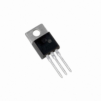
MJE13009 ON Semiconductor, MJE13009 Datasheet - Page 3

MJE13009
Manufacturer Part Number
MJE13009
Description
TRANS PWR NPN 12A 400V TO220AB
Manufacturer
ON Semiconductor
Datasheet
1.MJE13009.pdf
(10 pages)
Specifications of MJE13009
Transistor Type
NPN
Current - Collector (ic) (max)
12A
Voltage - Collector Emitter Breakdown (max)
400V
Vce Saturation (max) @ Ib, Ic
3V @ 3A, 12A
Dc Current Gain (hfe) (min) @ Ic, Vce
8 @ 5A, 5V
Power - Max
2W
Frequency - Transition
4MHz
Mounting Type
Through Hole
Package / Case
TO-220-3 (Straight Leads)
Lead Free Status / RoHS Status
Contains lead / RoHS non-compliant
Current - Collector Cutoff (max)
-
Other names
MJE13009OS
Available stocks
Company
Part Number
Manufacturer
Quantity
Price
Part Number:
MJE13009
Manufacturer:
SI深爱
Quantity:
20 000
Part Number:
MJE13009-2
Manufacturer:
FAIRCHILD/仙童
Quantity:
20 000
Part Number:
MJE13009A
Manufacturer:
SI深爱
Quantity:
20 000
Company:
Part Number:
MJE13009G
Manufacturer:
ON Semiconductor
Quantity:
2
Company:
Part Number:
MJE13009H2
Manufacturer:
NPC
Quantity:
600
The Safe Operating Area figures shown in Figures 1 and 2 are specified ratings for these devices under the test conditions shown.
0.05
0.02
0.01
100
0.8
0.6
0.4
0.2
0.5
0.2
0.1
50
20
10
1
0
0.07
0.05
0.03
0.02
0.01
5
2
1
0.7
0.5
0.3
0.2
0.1
20
1
0.01
5
Figure 1. Forward Bias Safe Operating Area
7
0.01
D = 0.5
Figure 3. Forward Bias Power Derating
T
C
40
CURVES APPLY BELOW RATED
V
0.05
0.02
0.2
0.1
0.02
= 25°C
10
CE
, COLLECTOR−EMITTER VOLTAGE (VOLTS)
SINGLE PULSE
THERMAL LIMIT
BONDING WIRE LIMIT
SECOND BREAKDOWN LIM-
IT
T
60
DERATING
THERMAL
C
20
, CASE TEMPERATURE (°C)
0.05
V
CEO
dc
30
80
0.1
50
100
1 m
70 100
DOWN DERATING
s
SECOND BREAK-
0.2
Figure 4. Typical Thermal Response [Z
120
0.5
200
100 m
σ
140
300
http://onsemi.com
1
10 m
σ
160
MJE13009
500
2
t, TIME (ms)
3
Z
R
D CURVES APPLY FOR POWER
PULSE TRAIN SHOWN
READ TIME AT t
T
a transistor: average junction temperature and second
breakdown. Safe operating area curves indicate I
limits of the transistor that must be observed for reliable
operation; i.e., the transistor must not be subjected to greater
dissipation than the curves indicate.
variable depending on power level. Second breakdown
pulse limits are valid for duty cycles to 10% but must be
derated when T
not derate the same as thermal limitations. Allowable
current at the voltages shown on Figure 1 may be found at
any case temperature by using the appropriate curve on
Figure 3.
case temperatures, thermal limitations will reduce the power
that can be handled to values less than the limitations
imposed by second breakdown. Use of reverse biased safe
operating area data (Figure 2) is discussed in the applications
information section.
qJC(t)
J(pk)
qJC
There are two limitations on the power handling ability of
The data of Figure 1 is based on T
T
14
12
10
5
= 1.25°C/W MAX
8
6
4
2
0
J(pk)
− T
= r(t) R
0
C
= P
may be calculated from the data in Figure 4. At high
V
10
qJC
CEV
(pk)
Figure 2. Reverse Bias Switching Safe
100
1
, COLLECTOR−EMITTER CLAMP VOLTAGE (VOLTS)
Z
T
I
qJC(t)
B1
C
C
20
≤ 100°C
= 2.5 A
≥ 25_C. Second breakdown limitations do
qJC
200
(t)]
Operating Area
300
50
3 V
P
400
(pk)
DUTY CYCLE, D = t
100
1.5
V
t
1
500
t
2
200
C
= 25_C; T
5 V
600
V
BE(off)
1
/t
500
2
700
= 9 V
C
J(pk)
− V
1.0 k
800
CE
is


