2N5089RLRA ON Semiconductor, 2N5089RLRA Datasheet

TRANS SS NPN GP 25V 50MA TO-92

2N5089RLRA

Manufacturer Part Number
2N5089RLRA
Description
TRANS SS NPN GP 25V 50MA TO-92
Manufacturer
ON Semiconductor
Datasheet

Specifications of 2N5089RLRA

Transistor Type
NPN
Current - Collector (ic) (max)
50mA
Voltage - Collector Emitter Breakdown (max)
25V
Vce Saturation (max) @ Ib, Ic
500mV @ 1mA, 10mA
Dc Current Gain (hfe) (min) @ Ic, Vce
400 @ 100µA, 5V
Power - Max
625mW
Frequency - Transition
50MHz
Mounting Type
Through Hole
Package / Case
TO-92-3 (Standard Body), TO-226
Lead Free Status / RoHS Status
Contains lead / RoHS non-compliant
Current - Collector Cutoff (max)
-
2N5088, 2N5089
Amplifier Transistors
NPN Silicon
Features
Stresses exceeding Maximum Ratings may damage the device. Maximum
Ratings are stress ratings only. Functional operation above the Recommended
Operating Conditions is not implied. Extended exposure to stresses above the
Recommended Operating Conditions may affect device reliability.
1. R
*For additional information on our Pb−Free strategy and soldering details, please
MAXIMUM RATINGS
THERMAL CHARACTERISTICS
© Semiconductor Components Industries, LLC, 2006
March, 2006 − Rev. 3
Collector − Emitter Voltage
Collector − Base Voltage
Emitter − Base Voltage
Collector Current − Continuous
Total Device Dissipation @ T
Derate above 25°C
Total Device Dissipation @ T
Derate above 25°C
Operating and Storage Junction
Temperature Range
Thermal Resistance, Junction−to−Ambient
(Note 1)
Thermal Resistance, Junction−to−Case
download the ON Semiconductor Soldering and Mounting Techniques
Reference Manual, SOLDERRM/D.
Pb−Free Packages are Available*
qJA
is measured with the device soldered into a typical printed circuit board.
Characteristic
Rating
A
C
= 25°C
= 25°C
2N5088
2N5089
2N5088
2N5089
Symbol
Symbol
T
V
V
V
R
R
J
P
P
, T
CEO
CBO
EBO
I
qJA
qJC
C
D
D
stg
−55 to +150
Value
Max
83.3
625
200
3.0
5.0
1.5
30
25
35
30
50
12
1
mW/°C
mW/°C
mAdc
°C/W
°C/W
Unit
Unit
Vdc
Vdc
Vdc
mW
°C
W
2N5088
2N5088G
2N5088RLRA
2N5088RLRAG
2N5089
2N5089G
2N2089RLRA
2N2089RLRAG
2N2089RLRE
2N2089RLREG
†For information on tape and reel specifications,
including part orientation and tape sizes, please
refer to our Tape and Reel Packaging Specifications
Brochure, BRD8011/D.
1
Device
2
(Note: Microdot may be in either location)
3
ORDERING INFORMATION
2N508x = Device Code
A
Y
WW
G
BASE
http://onsemi.com
2
CASE 29
STYLE 1
= Assembly Location
= Year
= Work Week
= Pb−Free Package
(Pb−Free)
(Pb−Free)
(Pb−Free)
(Pb−Free)
(Pb−Free)
Package
TO−92
TO−92
TO−92
TO−92
TO−92
TO−92
TO−92
TO−92
TO−92
TO−92
TO−92
x = 8 or 9
Publication Order Number:
3 COLLECTOR
1 EMITTER
2000/Tape & Reel
2000/Tape & Reel
2000/Tape & Reel
2000/Tape & Reel
2000/Tape & Reel
2000/Tape & Reel
5000 Units/Box
5000 Units/Box
5000 Units/Box
5000 Units/Box
MARKING
DIAGRAM
Shipping
AYWW G
508x
2N
G
2N5088/D

Related parts for 2N5089RLRA

2N5089RLRA Summary of contents

Page 1

... Pb−Free strategy and soldering details, please download the ON Semiconductor Soldering and Mounting Techniques Reference Manual, SOLDERRM/D. © Semiconductor Components Industries, LLC, 2006 March, 2006 − Rev. 3 ...

Page 2

ELECTRICAL CHARACTERISTICS Characteristic OFF CHARACTERISTICS Collector −Emitter Breakdown Voltage (Note 1.0 mAdc Collector −Base Breakdown Voltage = 100 mAdc Collector Cutoff Current ( Vdc, ...

Page 3

BANDWIDTH = 1 ≈ 3 1.0 mA 7.0 5.0 300 mA 3 100 200 500 ...

Page 4

2.0 1.0 0.7 0.5 0.4 0.3 0.2 0.01 0.02 0.03 0.05 1 25°C J 0 0.4 0 ...

Page 5

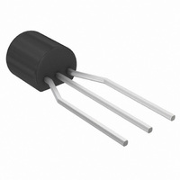
... CASE 29−11 ISSUE SECTION X−X N. American Technical Support: 800−282−9855 Toll Free USA/Canada Japan: ON Semiconductor, Japan Customer Focus Center 2−9−1 Kamimeguro, Meguro−ku, Tokyo, Japan 153−0051 Phone: 81−3−5773−3850 http://onsemi.com 5 NOTES: 1. DIMENSIONING AND TOLERANCING PER ANSI Y14 ...

Related keywords