BUV22 ON Semiconductor, BUV22 Datasheet

TRANS NPN 250V 40A BIPO TO-3

BUV22

Manufacturer Part Number
BUV22
Description
TRANS NPN 250V 40A BIPO TO-3
Manufacturer
ON Semiconductor
Series
SWITCHMODE™r
Datasheet

Specifications of BUV22

Transistor Type
NPN
Current - Collector (ic) (max)
40A
Voltage - Collector Emitter Breakdown (max)
250V
Vce Saturation (max) @ Ib, Ic
1.5V @ 2.5A, 20A
Current - Collector Cutoff (max)
3mA
Dc Current Gain (hfe) (min) @ Ic, Vce
20 @ 10A, 4V
Power - Max
250W
Frequency - Transition
8MHz
Mounting Type
Chassis Mount
Package / Case
TO-204, TO-3
Lead Free Status / RoHS Status
Contains lead / RoHS non-compliant

Available stocks

Company
Part Number
Manufacturer
Quantity
Price
Part Number:
BUV22
Manufacturer:
M
Quantity:
6
Part Number:
BUV22
Manufacturer:
ST
0
BUV22
SWITCHMODEt Series
NPN Silicon Power
Transistor
applications.
Features
Maximum ratings are those values beyond which device damage can occur.
Maximum ratings applied to the device are individual stress limit values (not
normal operating conditions) and are not valid simultaneously. If these limits are
exceeded, device functional operation is not implied, damage may occur and
reliability may be affected.
*For additional information on our Pb−Free strategy and soldering details, please
MAXIMUM RATINGS
THERMAL CHARACTERISTICS
© Semiconductor Components Industries, LLC, 2006
February, 2006 − Rev. 10
download the ON Semiconductor Soldering and Mounting Techniques
Reference Manual, SOLDERRM/D.
Collector−Emitter Voltage
Collector−Base Voltage
Emitter−Base Voltage
Collector−Emitter Voltage (V
Collector−Emitter Voltage (R
Collector−Current − Continuous
Base−Current Continuous
Total Device Dissipation @ T
Operating and Storage Junction
Temperature Range
Thermal Resistance, Junction−to−Case
This device is designed for high speed, high current, high power
High DC Current Gain:
Low V
Very Fast Switching Times:
Pb−Free Package is Available*
h
max = 1.0 V at I
TF max = 0.35 ms at I
FE
CE(sat)
min = 20 at I
Characteristics
, V
Rating
− Peak (PW v 10 ms)
CE(sat)
C
C
= 10 A
BE
BE
C
= 10 A
= 25_C
= −1.5 V)
= 100 W)
C
= 20 A
V
Symbol
Symbol
T
CEO(SUS)
V
V
V
V
J
I
q
P
CBO
, T
EBO
CEX
CER
CM
I
I
JC
C
B
D
stg
−65 to 200
Value
Max
250
300
300
290
250
0.7
40
50
7
8
1
_C/W
Unit
Unit
Vdc
Vdc
Vdc
Vdc
Vdc
Adc
Apk
Adc
_C
W
BUV22
BUV22G
Device
250 VOLTS − 250 WATTS
NPN SILICON POWER
METAL TRANSISTOR
ORDERING INFORMATION
BUV22 = Device Code
G
A
Y
WW
MEX
MARKING DIAGRAM
http://onsemi.com
40 AMPERES
TO−204AE (TO−3)
(Pb−Free)
Package
TO−204
TO−204
= Pb−Free Package
= Assembly Location
= Year
= Work Week
= Country of Origin
CASE 197A
BUV22G
AYWW
MEX
Publication Order Number:
100 Units / Tray
100 Units / Tray
Shipping
BUV22/D

Related parts for BUV22

BUV22 Summary of contents

Page 1

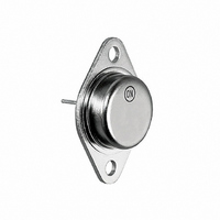
... BUV22G 1 http://onsemi.com 40 AMPERES NPN SILICON POWER METAL TRANSISTOR 250 VOLTS − 250 WATTS TO−204AE (TO−3) CASE 197A MARKING DIAGRAM BUV22G AYWW MEX BUV22 = Device Code G = Pb−Free Package A = Assembly Location Y = Year WW = Work Week MEX = Country of Origin ORDERING INFORMATION Device Package Shipping TO− ...

Page 2

... Fall Time Î Î Î Î Î Î Î Î Î Î Î Î Î Î Î Î Î Î Î Î Î Î 1. Pulse Test: Pulse Width v 300 ms, Duty Cycle v 2%. BUV22 (T = 25_C unless otherwise noted ...

Page 3

... I , COLLECTOR CURRENT (A) C Figure 5. Resistive Switching Performance BUV22 There are two limitations on the power handling ability of a transistor: average junction temperature and second breakdown. Safe operating area curves indicate I limits of the transistor that must be observed for reliable operation i.e., the transistor must not be subjected to greater dissipation than the curves indicate ...

Page 4

... L 0.665 BSC 16.89 BSC N 0.760 0.830 19.31 21.08 Q 0.151 0.165 3.84 4.19 U 1.187 BSC 30.15 BSC V 0.131 0.188 3.33 4.77 ON Semiconductor Website: http://onsemi.com Order Literature: http://www.onsemi.com/litorder For additional information, please contact your local Sales Representative. BUV22/D ...

Related keywords