MJ15001 ON Semiconductor, MJ15001 Datasheet
MJ15001
Specifications of MJ15001
Available stocks


Related parts for MJ15001

MJ15001 Summary of contents
Page 1
... MJ15001 (NPN), MJ15002 (PNP) Complementary Silicon Power Transistors The MJ15001 and MJ15002 are EpiBaset power transistors designed for high power audio, disk head positioners and other linear applications. Features • High Safe Operating Area (100% Tested) − 5 • For Low Distortion Complementary Designs • ...
Page 2
... V , COLLECTOR−EMITTER VOLTAGE (VOLTS) CE Figure 1. Active−Region Safe Operating Area MJ15001 (NPN), MJ15002 (PNP 25°C unless otherwise noted) C Characteristic = 150° 0.5 MHz) There are two limitations on the power handling ability of a transistor: average junction temperature and second breakdown. Safe operating area curves indicate I limits of the transistor that must be observed for reliable operation ...
Page 3
... MJ15001 (NPN), MJ15002 (PNP) 1000 700 C 500 ib 300 C ib 200 100 MJ15001 (NPN) MJ15002 (PNP 1 REVERSE VOLTAGE (VOLTS) R Figure 2. Capacitances MJ15001 200 T = 100°C J 100 25° 0.2 0.3 0.5 0 COLLECTOR CURRENT (AMP) C MJ15001 2.0 1.6 1 Vdc 25° 100° ...
Page 4
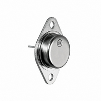
... P.O. Box 61312, Phoenix, Arizona 85082−1312 USA Phone: 480−829−7710 or 800−344−3860 Toll Free USA/Canada Fax: 480−829−7709 or 800−344−3867 Toll Free USA/Canada Email: orderlit@onsemi.com MJ15001 (NPN), MJ15002 (PNP) PACKAGE DIMENSIONS TO−204 (TO−3) CASE 1−07 ISSUE Z SEATING − ...