MPSA28RLRP ON Semiconductor, MPSA28RLRP Datasheet

TRANS NPN DARL BIPO 80V TO-92

MPSA28RLRP

Manufacturer Part Number
MPSA28RLRP
Description
TRANS NPN DARL BIPO 80V TO-92
Manufacturer
ON Semiconductor
Datasheet

Specifications of MPSA28RLRP

Transistor Type
NPN - Darlington
Current - Collector (ic) (max)
500mA
Voltage - Collector Emitter Breakdown (max)
80V
Vce Saturation (max) @ Ib, Ic
1.5V @ 100µA, 100mA
Current - Collector Cutoff (max)
500nA
Dc Current Gain (hfe) (min) @ Ic, Vce
10000 @ 100mA, 5V
Power - Max
625mW
Frequency - Transition
200MHz
Mounting Type
Through Hole
Package / Case
TO-92-3 (Standard Body), TO-226
Lead Free Status / RoHS Status
Contains lead / RoHS non-compliant
MPSA28, MPSA29
Darlington Transistors
NPN Silicon
Features
Maximum ratings are those values beyond which device damage can occur.
Maximum ratings applied to the device are individual stress limit values (not
normal operating conditions) and are not valid simultaneously. If these limits are
exceeded, device functional operation is not implied, damage may occur and
reliability may be affected.
*For additional information on our Pb−Free strategy and soldering details, please
© Semiconductor Components Industries, LLC, 2006
January, 2006 − Rev. 2
MAXIMUM RATINGS
THERMAL CHARACTERISTICS
download the ON Semiconductor Soldering and Mounting Techniques
Reference Manual, SOLDERRM/D.
Collector −Emitter Voltage
Collector −Base Voltage
Emitter −Base Voltage
Collector Current − Continuous
Total Device Dissipation @ T
Derate above 25°C
Total Device Dissipation @ T
Derate above 25°C
Operating and Storage Junction
Temperature Range
Thermal Resistance, Junction−to−Ambient
Thermal Resistance, Junction−to−Case
Pb−Free Packages are Available*
Characteristic
Rating
MPSA29 is a Preferred Device
A
C
= 25°C
= 25°C
MPSA28
MPSA29
MPSA28
MPSA29
Symbol
Symbol
T
V
V
V
R
R
J
P
P
CBO
EBO
, T
CES
I
qJA
qJC
C
D
D
stg
−55 to +150
Value
Max
83.3
100
100
500
625
200
5.0
1.5
80
80
12
12
1
mW/°C
mW/°C
mAdc
°C/W
°C/W
Unit
Unit
Vdc
Vdc
Vdc
mW
°C
W
MPSA28
MPSA28G
MPSA28RLRP
MPSA28RLRPG
MPSA29
MPSA29G
MPSA29RLRP
MPSA29RLRPG
Preferred devices are recommended choices for future use
and best overall value.
1
Device
2
(Note: Microdot may be in either location)
3
MPSA2x = Device Code
A
Y
WW
G
ORDERING INFORMATION
BASE
2
http://onsemi.com
CASE 29−11
COLLECTOR 3
= Assembly Location
= Year
= Work Week
= Pb−Free Package
EMITTER 1
STYLE 1
(Pb−Free)
(Pb−Free)
(Pb−Free)
(Pb−Free)
Package
TO−92
TO−92
TO−92
TO−92
TO−92
TO−92
TO−92
TO−92
TO−92
x = 8 or 9
Publication Order Number:
2,000/Ammo Pack
2,000/Ammo Pack
2,000/Ammo Pack
2,000/Ammo Pack
5,000 Units/Box
5,000 Units/Box
5,000 Units/Box
5,000 Units/Box
MARKING
DIAGRAM
Shipping
AYWW G
MPS
MPSA28/D
A2x
G

Related parts for MPSA28RLRP

MPSA28RLRP Summary of contents

Page 1

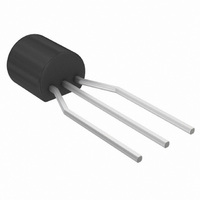
... J stg Symbol Max Unit °C/W 200 R qJA °C/W 83.3 R qJC MPSA28 MPSA28G MPSA28RLRP MPSA28RLRPG MPSA29 MPSA29G MPSA29RLRP MPSA29RLRPG Preferred devices are recommended choices for future use and best overall value. 1 http://onsemi.com COLLECTOR 3 BASE 2 EMITTER 1 MARKING DIAGRAM MPS A2x AYWW G TO− ...

Page 2

ELECTRICAL CHARACTERISTICS Characteristic OFF CHARACTERISTICS Collector −Emitter Breakdown Voltage = 100 mAdc Collector −Base Breakdown Voltage = 100 mAdc Emitter −Base Breakdown Voltage = 10 mAdc ...

Page 3

200 T = 125°C A 100 T = 25° −55° 5.0 2.0 1.0 1.0 2.0 5 100 I , COLLECTOR CURRENT (mA) C Figure 1. ...

Page 4

... ISSUE SECTION X−X N. American Technical Support: 800−282−9855 Toll Free USA/Canada Japan: ON Semiconductor, Japan Customer Focus Center 2−9−1 Kamimeguro, Meguro−ku, Tokyo, Japan 153−0051 Phone: 81−3−5773−3850 http://onsemi.com 4 NOTES: 1. DIMENSIONING AND TOLERANCING PER ANSI Y14.5M, 1982. ...

Related keywords