DDTC143ZLP-7 Diodes Inc, DDTC143ZLP-7 Datasheet

TRANS PREBIASED NPN 3-DFN

DDTC143ZLP-7

Manufacturer Part Number
DDTC143ZLP-7
Description
TRANS PREBIASED NPN 3-DFN
Manufacturer
Diodes Inc
Datasheet

Specifications of DDTC143ZLP-7

Transistor Type
NPN - Pre-Biased
Current - Collector (ic) (max)
100mA
Voltage - Collector Emitter Breakdown (max)
50V
Resistor - Base (r1) (ohms)
4.7K
Resistor - Emitter Base (r2) (ohms)
47K
Dc Current Gain (hfe) (min) @ Ic, Vce
180 @ 50mA, 5V
Vce Saturation (max) @ Ib, Ic
200mV @ 5mA, 50mA
Current - Collector Cutoff (max)
500nA
Frequency - Transition
250MHz
Power - Max
250mW
Mounting Type
Surface Mount
Package / Case
3-DFN
Lead Free Status / RoHS Status
Lead free / RoHS Compliant
Other names
DDTC143ZLPDITR

Available stocks

Company
Part Number
Manufacturer
Quantity
Price
Part Number:
DDTC143ZLP-7
Manufacturer:
Diodes Inc.
Quantity:
37 530
Maximum Ratings
Thermal Characteristics
Supply Voltage
Input Voltage
Output Voltage
Maximum Collector Current
Power Dissipation (Note 3)
Power Deration above 25 °C
Thermal Resistance, Junction to Ambient Air (Note 3)
(Equivalent to one heated junction of NPN)
Operating and Storage Temperature Range
Features
Notes:
DDTCxxxxLP (R1≠R2 Series)
Document number: DS30755 Rev. 7 - 2
Part Number
DDTC114YLP
DDTC123JLP
DDTC143ZLP
Epitaxial Planar Die Construction
Ultra-Small Leadless Surface Mount Package
Ideally Suited for Automated Assembly Processes
Lead Free By Design/RoHS Compliant (Note 1)
"Green" Device (Note 2)
Qualified to AEC-Q101 Standards for High Reliability
1.
2.
3.
Characteristic
No purposefully added lead.
Diodes Inc.'s "Green" policy can be found on our website at http://www.diodes.com/products/lead_free/index.php.
Device mounted on FR-4 PCB, 1 inch x 0.85 inch x 0.062 inch; pad layout as shown on Diodes Inc. suggested pad layout document AP02001, which
can be found on page 6 or our website at http://www.diodes.com/datasheets/ap02001.pdf.
Characteristic
Bottom View
R1 (NOM)
2.2K
4.7K
10K
@T
A
= 25°C unless otherwise specified
3
PRE-BIASED SMALL SIGNAL SURFACE MOUNT 100mA NPN TRANSISTOR
C
Package Pin Out
Configuration
R2 (NOM)
DDTC143ZLP
DDTC114YLP
DDTC143ZLP
DDTC114YLP
DDTC123JLP
DDTC123JLP
R
1
47K
47K
47K
R
P/N
2
1
2
E
B
www.diodes.com
Symbol
T
J
R
P
, T
P
θ JA
der
D
STG
1 of 7
IN
Mechanical Data
1
Symbol
I
Please click here to visit our online spice models database.
B
C(MAX)
V
V
I
Case: DFN1006-3
Case Material: Molded Plastic, "Green" Molding Compound.
UL Flammability Classification Rating 94V-0
Moisture Sensitivity: Level 1 per J-STD-020D
Terminal Connections: Collector Dot (See Diagram and
Marking Information)
Terminals: Finish ⎯ NiPdAu over Copper leadframe.
Solderable per MIL-STD-202, Method 208
Marking Information: See Page 6
Ordering Information: See Page 6
Weight: 0.0009 grams (approximate)
CC
O
2
IN
E
GND
C
3
-55 to +150
OUT
Device Schematics
Value
DDTCxxxxLP (R1≠R2 Series)
250
500
2
-5 to +12
-5 to +30
-5 to +40
Value
100
100
100
50
70
IN
1
R
1
R
2
B
mW/°C
C
°C/W
Unit
mW
E
© Diodes Incorporated
°C
3
2
Unit
OUT
mA
mA
GND
V
V
March 2009

Related parts for DDTC143ZLP-7

DDTC143ZLP-7 Summary of contents

Page 1

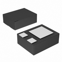
... Ordering Information: See Page 6 • 47K Weight: 0.0009 grams (approximate GND Package Pin Out Configuration P/N Symbol V CC DDTC123JLP DDTC143ZLP V IN DDTC114YLP DDTC123JLP DDTC143ZLP I O DDTC114YLP I C(MAX) Symbol der R θ STG www.diodes.com DDTCxxxxLP (R1≠R2 Series OUT OUT GND ...

Page 2

... DDTC123JLP Base-Emitter Turn-On Voltage* DDTC143ZLP DDTC114YLP DDTC123JLP Base-Emitter Saturation Voltage* DDTC143ZLP DDTC114YLP Input-On Voltage DDTC123JLP Input Current DDTC143ZLP DDTC114YLP DC Current Gain Collector-Emitter Saturation Voltage Output On Voltage (Same CE(SAT) Input Resistor +/-30% Resistor Ratio Small Signal Characteristics Transition Frequency (gain bandwidth product) *Guaranteed by design Notes: 4 ...

Page 3

... I , COLLECTOR CURRENT (mA) C Fig. 3 Typical Collector Emitter Saturation Voltage vs. Collector Current 5mA O - 120 ° AMBIENT TEMPERATURE ( ° 150 C ° - ° COLLECTOR CURRENT (mA) C Fig. 7 Typical Base Emitter Saturation Voltage vs. Collector Current © Diodes Incorporated ° 100 150 ° 100 March 2009 ...

Page 4

... Characteristics Curves of DDTC143ZLP 350 ° 150 C 300 A ° 250 200 150 100 COLLECTOR CURRENT (mA) C Fig. 8 Typical DC Current Gain vs. Collector Current 0.05 0.04 0.03 0.02 0. 0.5 1 1 COLLECTOR EMITTER VOLTAGE (V) CE Fig. 10 Typical Collector Current vs. Collector Emitter Voltage ° ...

Page 5

... I , COLLECTOR CURRENT (mA) C Fig. 15 Typical Collector Emitter Saturation Voltage vs. Collector Current 5mA O - 120 ° AMBIENT TEMPERATURE ( ° ° 150 C A ° - ° COLLECTOR CURRENT (mA) C Fig. 19 Typical Base Emitter Saturation Voltage vs. Collector Current © Diodes Incorporated 100 150 100 March 2009 ...

Page 6

... Ordering Information (Note 5) Part Number DDTC123JLP-7 DDTC143ZLP-7 DDTC114YLP-7 Notes: 5. For packaging details our website at http://www.diodes.com/datasheets/ap02007.pdf. Marking Information Package Outline Dimensions Suggested Pad Layout DDTCxxxxLP (R1≠R2 Series) Document number: DS30755 Rev Case DFN1006-3 DFN1006-3 DFN1006 Product Type Marking Code: DDTC123JLP = N0 Nx ...

Page 7

... Any Customer or user of this document or products described herein in such applications shall assume all risks of such use and will agree to hold Diodes Incorporated and all the companies whose products are represented on Diodes Incorporated website, harmless against all damages. ...

Related keywords