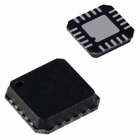
ADG788BCPZ Analog Devices Inc, ADG788BCPZ Datasheet - Page 10

ADG788BCPZ
Manufacturer Part Number
ADG788BCPZ
Description
Analog Switch Quad SPDT 20-Pin LFCSP EP
Manufacturer
Analog Devices Inc
Type
Analog Switchr
Datasheet
1.ADG788BCPZ.pdf
(12 pages)
Specifications of ADG788BCPZ
Function
Switch
Circuit
4 x SPDT
On-state Resistance
4.5 Ohm
Voltage Supply Source
Single, Dual Supply
Voltage - Supply, Single/dual (±)
1.8 V ~ 5.5 V, ±2.5 V
Current - Supply
0.001µA
Operating Temperature
-40°C ~ 85°C
Mounting Type
Surface Mount
Package / Case
20-VFQFN, CSP Exposed Pad
Package/case
20-CSP
Leakage Current
100nA
On-resistance, Rds(on)
2.5mOhm
Number Of Circuits
4
Rohs Compliant
Yes
No. Of Channels
4
Bandwidth
160MHz
On State Resistance Max
5ohm
Turn Off Time
7ns
Turn On Time
19ns
Supply Voltage Range
1.8V To 5.5V
Operating Temperature Range
-40°C To +85°C
Multiplexer Configuration
Quad SPDT
Number Of Inputs
4
Number Of Outputs
8
Number Of Channels
4
Analog Switch On Resistance
11@3VOhm
Analog Switch Turn On Time
28ns
Analog Switch Turn Off Time
10ns
Package Type
LFCSP
Power Supply Requirement
Single/Dual
Single Supply Voltage (min)
1.8V
Single Supply Voltage (typ)
3/5V
Single Supply Voltage (max)
5.5V
Dual Supply Voltage (typ)
±2.5V
Power Dissipation
0.000005W
Supply Current
0.001mA
Mounting
Surface Mount
Pin Count
20
Operating Temp Range
-40C to 85C
Operating Temperature Classification
Industrial
Lead Free Status / RoHS Status
Lead free / RoHS Compliant
For Use With
EVAL-ADG788EBZ - BOARD EVALUATION FOR ADG788
Lead Free Status / Rohs Status
Compliant
Available stocks
Company
Part Number
Manufacturer
Quantity
Price
Company:
Part Number:
ADG788BCPZ
Manufacturer:
ADI
Quantity:
218
Part Number:
ADG788BCPZ
Manufacturer:
ADI/亚德诺
Quantity:
20 000
ADG786/ADG788
V
OUT
ANALYZER
NETWORK
V
IN
IN
0.1 F
50
V
S
R
50
L
V
V
DD
DD
GND
S
V
D
R
V
V
SS
S
S
SS
0.1 F
V
IN
IN
* IN1–4 for ADG734
0.1 F
50
V
OFF ISOLATION = 20 LOG
SA
SB
V
DD
S
EN*
DD
V
V
DD
DD
ADG786/
ADG788
GND
GND
V
V
CHANNEL-TO-CHANNEL
CROSSTALK = 20 LOG
SS
SS
V
V
0.1 F
SS
SS
50
R
ANALYZER
NETWORK
50
D
L
D
V
OUT
V
S
50
R
V
OUT
V
C
1nF
S
L
V
OUT
V
V
S
OUT
INPUT (V
Power Supply Sequencing
When using CMOS devices, care must be taken to ensure cor-
rect power supply sequencing. Incorrect sequencing can result
in the device being subjected to stresses beyond those maximum
ratings listed in the data sheet. Digital and analog inputs should
be applied to the device after supplies and ground. In dual sup-
ply applications, if digital and analog inputs may be applied
prior to V
connected between V
powers on correctly. For single supply applications, V
be tied to GND as close to the device as possible.
LOGIC
V
IN
OUT
3V
0V
)
V
IN
IN
0.1 F
DD
V
and V
V
DD
DD
GND
S
INSERTION LOSS = 20 LOG
SS
Q
V
D
V
INJ
SS
SS
SS
supplies, the addition of a Schottky diode
0.1 F
= C
and GND will ensure that the device
L
V
OUT
V
OUT
V
OUT
V
OUT
50
R
ANALYZER
NETWORK
WITHOUT SWITCH
50
L
WITH SWITCH
V
OUT
V
S
SS
should


