BTA08-800BW3G ON Semiconductor, BTA08-800BW3G Datasheet

TRIAC ISO 8A 800V TO220AB

BTA08-800BW3G

Manufacturer Part Number
BTA08-800BW3G
Description
TRIAC ISO 8A 800V TO220AB
Manufacturer
ON Semiconductor
Datasheet

Specifications of BTA08-800BW3G

Triac Type
Standard
Mounting Type
Through Hole
Configuration
Single
Current - Hold (ih) (max)
60mA
Voltage - Off State
800V
Current - Gate Trigger (igt) (max)
50mA
Current - Non Rep. Surge 50, 60hz (itsm)
90A @ 60Hz
Current - On State (it (rms)) (max)
8A
Voltage - Gate Trigger (vgt) (max)
1.1V
Package / Case
TO-220-3
Current - On State (it (rms) (max)
8A
Lead Free Status / RoHS Status
Lead free / RoHS Compliant
BTA08-600BW3G,
BTA08-800BW3G
Triacs
Silicon Bidirectional Thyristors
where high noise immunity and high commutating di/dt are required.
Features
Stresses exceeding Maximum Ratings may damage the device. Maximum
Ratings are stress ratings only. Functional operation above the Recommended
Operating Conditions is not implied. Extended exposure to stresses above the
Recommended Operating Conditions may affect device reliability.
1. V
MAXIMUM RATINGS
August, 2008 − Rev. 0
Peak Repetitive Off−State Voltage (Note 1)
(T
50 to 60 Hz, Gate Open)
On-State RMS Current
(Full Cycle Sine Wave, 60 Hz, T
Peak Non-Repetitive Surge Current
(One Full Cycle Sine Wave, 60 Hz,
T
Circuit Fusing Consideration (t = 8.3 ms)
Non−Repetitive Surge Peak Off−State
Voltage (T
Peak Gate Current (T
Peak Gate Power
(Pulse Width
Average Gate Power (T
Operating Junction Temperature Range
Storage Temperature Range
RMS Isolation Voltage
(t = 300 ms, R.H.
Designed for high performance full-wave ac control applications
C
Blocking Voltage to 800 V
On-State Current Rating of 8 A RMS at 80 C
Uniform Gate Trigger Currents in Three Quadrants
High Immunity to dV/dt − 2000 V/ms minimum at 125 C
Minimizes Snubber Networks for Protection
Industry Standard TO-220AB Package
High Commutating dI/dt − 1.5 A/ms minimum at 125 C
Internally Isolated (2500 V
These are Pb−Free Devices
Semiconductor Components Industries, LLC, 2008
voltages shall not be tested with a constant current source such that the
voltage ratings of the devices are exceeded.
J
= 25 C)
DRM
= −40 to 125 C, Sine Wave,
and V
J
= 25 C, t = 10ms)
RRM
1.0 ms, T
Rating
for all types can be applied on a continuous basis. Blocking
30%, T
J
= 125 C, t = 20ms)
J
BTA08−600BW3G
BTA08−800BW3G
(T
C
= 125 C)
= 80 C)
J
A
= 25 C unless otherwise noted)
= 25 C)
C
RMS
= 80 C)
)
Symbol
I
P
V
V
V
T(RMS)
V
I
P
I
T
V
TSM
G(AV)
DRM,
DSM/
RRM
RSM
I
GM
T
GM
stg
2
iso
J
t
V
−40 to +125
−40 to +150
DSM/
Value
+100
2500
600
800
8.0
4.0
1.0
90
36
20
V
RSM
1
A
Unit
2
W
W
V
A
A
V
A
V
sec
C
C
*For additional information on our Pb−Free strategy and
BTA08−600BW3G
BTA08−800BW3G
soldering details, please download the ON Semicon-
ductor Soldering and Mounting Techniques Reference
Manual, SOLDERRM/D.
1
2
x
A
Y
WW
G
3
1
2
3
4
Device
MT2
ORDERING INFORMATION
600 thru 800 VOLTS
8 AMPERES RMS
4
= 6 or 8
= Assembly Location
= Year
= Work Week
= Pb−Free Package
http://onsemi.com
PIN ASSIGNMENT
CASE 221A
TO−220AB
STYLE 12
TRIACS
TO−220AB
TO−220AB
(Pb−Free)
(Pb−Free)
Package
Main Terminal 1
Main Terminal 2
Publication Order Number:
No Connection
Gate
BTA08−600BW3/D
BTA08−xBWG
G
MARKING
DIAGRAM
50 Units / Rail
50 Units / Rail
MT1
AYWW
Shipping

Related parts for BTA08-800BW3G

BTA08-800BW3G Summary of contents

Page 1

... BTA08-600BW3G, BTA08-800BW3G Triacs Silicon Bidirectional Thyristors Designed for high performance full-wave ac control applications where high noise immunity and high commutating di/dt are required. Features Blocking Voltage to 800 V On-State Current Rating RMS Uniform Gate Trigger Currents in Three Quadrants High Immunity to dV/dt − 2000 V/ms minimum at 125 C ...

Page 2

THERMAL CHARACTERISTICS Characteristic Thermal Resistance, Junction−to−Case (AC) Junction−to−Ambient Maximum Lead Temperature for Soldering Purposes 1/8 from Case for 10 seconds ELECTRICAL CHARACTERISTICS Characteristic OFF CHARACTERISTICS Peak Repetitive Blocking Current (V = Rated Gate Open) D DRM ...

Page 3

... Voltage Current Characteristic of Triacs Symbol Parameter V Peak Repetitive Forward Off State Voltage DRM I Peak Forward Blocking Current DRM V Peak Repetitive Reverse Off State Voltage RRM I Peak Reverse Blocking Current RRM V Maximum On State Voltage TM I Holding Current H Quadrant II (−) I GATE I − GT Quadrant III (− ...

Page 4

DC 105 100 RMS ON-STATE CURRENT (A) T(RMS) Figure 1. RMS Current Derating 100 Typical @ T = − ...

Page 5

−40 −25 − JUNCTION TEMPERATURE ( C) J Figure 6. Gate Trigger Current Variation 5000 100 R , GATE TO MAIN TERMINAL 1 ...

Page 6

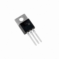
... U 0.000 0.050 0.00 1.27 V 0.045 --- 1.15 --- Z --- 0.080 --- 2.04 STYLE 12: PIN 1. MAIN TERMINAL 1 2. MAIN TERMINAL 2 3. GATE 4. NOT CONNECTED ON Semiconductor Website: www.onsemi.com Order Literature: http://www.onsemi.com/orderlit For additional information, please contact your local Sales Representative BTA08−600BW3/D ...

Related keywords