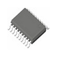
ICS8543BG IDT, Integrated Device Technology Inc, ICS8543BG Datasheet - Page 7

ICS8543BG
Manufacturer Part Number
ICS8543BG
Description
Manufacturer
IDT, Integrated Device Technology Inc
Type
Clock Driverr
Datasheet
1.ICS8543BG.pdf
(18 pages)
Specifications of ICS8543BG
Number Of Clock Inputs
2
Mode Of Operation
Differential
Output Frequency
800MHz
Output Logic Level
LVDS
Operating Supply Voltage (min)
3.135V
Operating Supply Voltage (typ)
3.3V
Operating Supply Voltage (max)
3.465V
Package Type
TSSOP
Operating Temp Range
0C to 70C
Operating Temperature Classification
Commercial
Mounting
Surface Mount
Pin Count
20
Lead Free Status / RoHS Status
Not Compliant
Available stocks
Company
Part Number
Manufacturer
Quantity
Price
Company:
Part Number:
ICS8543BG
Manufacturer:
ICS
Quantity:
365
Company:
Part Number:
ICS8543BG
Manufacturer:
ICSI
Quantity:
12 950
Company:
Part Number:
ICS8543BGILF
Manufacturer:
NUVOTON
Quantity:
5 000
Part Number:
ICS8543BGILFT
Manufacturer:
IDT
Quantity:
20 000
Company:
Part Number:
ICS8543BGLF
Manufacturer:
IDT
Quantity:
755
Part Number:
ICS8543BGLFT
Manufacturer:
IDT
Quantity:
20 000
ICS8543 Data Sheet
Additive Phase Jitter
The spectral purity in a band at a specific offset from the fundamental
compared to the power of the fundamental is called the dBc Phase
Noise. This value is normally expressed using a Phase noise plot
and is most often the specified plot in many applications. Phase noise
is defined as the ratio of the noise power present in a 1Hz band at a
specified offset from the fundamental frequency to the power value of
the fundamental. This ratio is expressed in decibels (dBm) or a ratio
As with most timing specifications, phase noise measurements has
issues relating to the limitations of the equipment. Often the noise
floor of the equipment is higher than the noise floor of the device. This
ICS8543BG REVISION E DECEMBER 17, 2010
Offset from Carrier Frequency (Hz)
7
of the power in the 1Hz band to the power in the fundamental. When
the required offset is specified, the phase noise is called a dBc value,
which simply means dBm at a specified offset from the fundamental.
By investigating jitter in the frequency domain, we get a better
understanding of its effects on the desired application over the entire
time record of the signal. It is mathematically possible to calculate an
expected bit error rate given a phase noise plot.
is illustrated above. The device meets the noise floor of what is
shown, but can actually be lower. The phase noise is dependent on
the input source and measurement equipment.
LOW SKEW, 1-to-4, DIFFERENTIAL-TO-LVDS FANOUT BUFFER
12kHz to 20MHz = 0.164ps (typical)
Additive Phase Jitter @ 153.6MHz
©2010 Integrated Device Technology, Inc.


