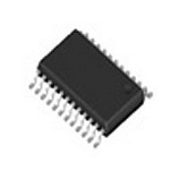
5T93GL04PGI8 IDT, Integrated Device Technology Inc, 5T93GL04PGI8 Datasheet - Page 12

5T93GL04PGI8
Manufacturer Part Number
5T93GL04PGI8
Description
Manufacturer
IDT, Integrated Device Technology Inc
Type
Clock Driverr
Datasheet
1.5T93GL04PGI8.pdf
(17 pages)
Specifications of 5T93GL04PGI8
Number Of Clock Inputs
2
Mode Of Operation
Differential
Output Frequency
450MHz
Output Logic Level
LVDS
Operating Supply Voltage (min)
2.3V
Operating Supply Voltage (typ)
2.5V
Operating Supply Voltage (max)
2.7V
Package Type
TSSOP
Operating Temp Range
-40C to 85C
Operating Temperature Classification
Industrial
Mounting
Surface Mount
Pin Count
24
Quiescent Current
240mA
Lead Free Status / RoHS Status
Not Compliant
IDT5T93GL04 Data Sheet
Power Down Timing
NOTE 1: It is recommended that outputs be disabled before entering power-down mode. It is also recommended that the outputs remain
disabled until the device completes power-up after asserting PD.
NOTE 2: The Power Down Timing diagram assumes that GL is HIGH.
NOTE 3: It should be noted that during power-down mode, the outputs are both pulled to V
shown when Qn/Qn goes to V
IDT5T93GL04 REVISION A OCTOBER 30, 2009
Qn - Qn
A
A
1
2
- A
- A
PD
G
1
2
DIF
= 0.
12
2.5V LVDS 1:4 GLITCHLESS CLOCK BUFFER TERABUFFER™ II
DD
. In the Power Down Timing diagram this is
+V
V
-V
+V
V
-V
+V
V
-V
V
V
V
V
V
V
DIF
DIF
DIF
THI
THI
IH
IL
IH
IL
DIF
DIF
DIF
DIF
DIF
DIF
=0
=0
=0
©2009 Integrated Device Technology, Inc.


