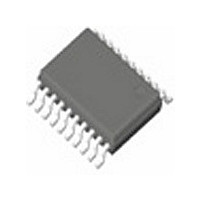
ICS8523BG IDT, Integrated Device Technology Inc, ICS8523BG Datasheet - Page 8

ICS8523BG
Manufacturer Part Number
ICS8523BG
Description
Manufacturer
IDT, Integrated Device Technology Inc
Type
Clock Driverr
Datasheet
1.ICS8523BG.pdf
(17 pages)
Specifications of ICS8523BG
Number Of Clock Inputs
2
Mode Of Operation
Differential
Output Frequency
650MHz
Output Logic Level
HSTL
Operating Supply Voltage (min)
3.135V
Operating Supply Voltage (typ)
3.3V
Operating Supply Voltage (max)
3.465V
Package Type
TSSOP
Operating Temp Range
0C to 70C
Operating Temperature Classification
Commercial
Mounting
Surface Mount
Pin Count
20
Lead Free Status / RoHS Status
Not Compliant
Available stocks
Company
Part Number
Manufacturer
Quantity
Price
Company:
Part Number:
ICS8523BG
Manufacturer:
SANYO
Quantity:
230
Company:
Part Number:
ICS8523BGI
Manufacturer:
PHILIPS
Quantity:
367
Company:
Part Number:
ICS8523BGLF
Manufacturer:
ICS
Quantity:
5 510
Parameter Measurement Information, continued
Output Duty Cycle/Pulse Width/Period
Application Information
Wiring the Differential Input to Accept Single Ended Levels
Figure 2 shows how the differential input can be wired to accept
single ended levels. The reference voltage V_REF = V
generated by the bias resistors R1, R2 and C1. This bias circuit
should be located as close as possible to the input pin. The ratio of
R1 and R2 might need to be adjusted to position the V_REF in the
center of the input voltage swing. For example, if the input clock
swing is only 2.5V and V
R2/R1 = 0.609.
IDT™ / ICS™ HSTL FANOUT BUFFER
ICS8523
LOW SKEW, 1-TO-4, DIFFERENTIAL-TO-HSTL FANOUT BUFFER
Qy
Qx
Qy
Qx
tsk(o)
DD
= 3.3V, V_REF should be 1.25V and
DD
/2 is
8
Figure 2. Single-Ended Signal Driving Differential Input
Single Ended Clock Input
C1
0.1u
V_REF
ICS8523CG REV. D MARCH 13, 2007
R1
1K
R2
1K
V
DD
CLK
nCLK


